Electronics Forum | Tue Aug 22 14:52:55 EDT 2000 | John Thorup
Jax - absolutely right - the archives are a valuable tool and deserve to be used more than they seem to be. Caumel - Are your blobs on the solder side or the component side? Are your vias tented on the component side? What size are your vias? Is th
Electronics Forum | Thu Sep 02 11:47:55 EDT 1999 | ScottM
| For space contracts we have to mount chip capacitors/ resistors etc 0.1 to 0.4 mm from the pad height. | | This is to compenstae for the CTE differential in the substrate/component and also to ensure cleanliness. | | Does anyone have any new idea
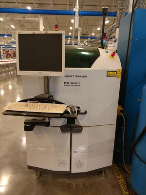
Used SMT Equipment | SPI / Solder Paste Inspection
Agilent SP50 Series II 3D SPI 3D Solder Paste Inspection System Model: SP50 Series II Vintage: 2006 Maximum board size: 510 by 510 mm (20 by 20 in) Minimum board size: 50 by 50 mm (1.97 by 1.97 in) Maximum board thickness: 4 mm (0.16 in) 2D an
Industry News | 2001-08-01 16:07:13.0
Image Processing Libraries Add Enhancements for Rapid Application Development and High-Speed Performance
GPD Global | https://www.gpd-global.com/co_website/pdf/doc/FLOware-Software-Guide-Addendum-Deferred-Reverse.pdf
(pixels) of blobs for blob search. Max Area Maximum area (pixels) of blobs for blob search. Window Height Window Width Used to determine the size of a search window for dot inspection. Establishing a narrow area only slightly larger than the dot to be found


