Industry Directory | Consultant / Service Provider / Manufacturer
Tropical Stencil is dedicated to providing the highest quality Laser Cut Stencils; with our rapid response, you will have your Stencil delivered on-time.
Industry Directory | Manufacturer
Supplier of High-Tech Low-Cost Printed Circuit Boards with 1-48 layers from 24h express. Flex, flex-rigid, metal core, impedance control, blind & buried vias as well as SMD Stencils.
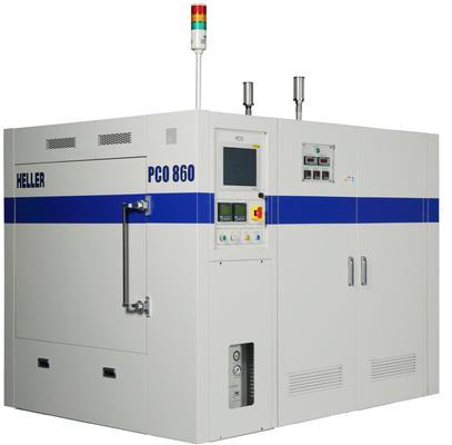
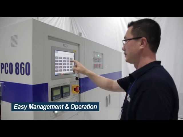
New Equipment | Curing Equipment
A Pressure Cure Oven (PCO), or Autoclave, is used to minimize voiding and increase adhesion strength for bonding processes typically used in die attach and underfill applications. PCO pressurizes air into a rigid vessel and heats & cools with
SMT Stencil Printer/ PCB Printers/ Solder Paste Stencil Printer Semi-Auto Main product: Stencil Printer, Semi-Automatic Printing, PCB Printer, screen printing, SMT Stencil Printer, SMT screen printer, SMT printer, Solder Paste Printer, SMT solder p
Electronics Forum | Wed Mar 27 16:54:47 EST 2002 | davef
STARTING RANGES * Pressure � 1 pound/inch of blade (metal); 1.6-3 pound/inch (plastic) * Speed - 0.5 to 3 inch per sec [for standard pitch]; 0.5 to 1 inch per sec [for fine pitch] Your paste supplier�s recommendation is a good place to start. * Sepa
Electronics Forum | Thu Jan 06 06:15:49 EST 2005 | mattkehoe
We need some opinions about a situation that is causing problems in our process. The pcb's in question are .125 thick with a HASL finish. The boards are coming in with a large amount of solder trapped inside the via holes. Sometimes this solder is ac
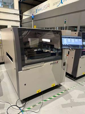
Used SMT Equipment | Screen Printers
EKRA X5 Professional Large, Screen and Stencil Printer Type: X5 Prof Large Serial Nr.: 805843 Year of Manufacture: 2014 Direction: Left to Right Voltage: 400V, 50/60Hz, 3 Phases Air Pressure: 6 Bar Printing Area: min.: 80x50mm, max.: 660x550mm Printe
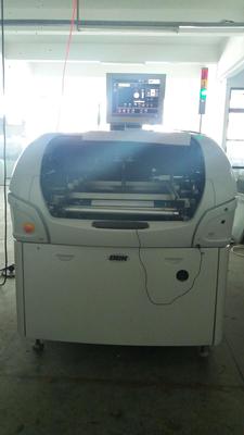
Used SMT Equipment | Screen Printers
HORIZON 02i Approx. Weight 820kg boxed 677kg unboxed Approx. Dimensions 2060mm x 1500mm x 1570mm (81.1” x 59” x 61.8”) Accuracy and Repeatability 1.6 Cpk @ +/- 25 m Cycle Core Time 12 seconds Max. Board Size (Print Area) 508mm (X) x 508mm (Y)
Industry News | 2003-03-11 08:45:00.0
CAMtastic DXP is the latest version of Altium's complete CAM verification and editing system that bridges the gap between PCB design and manufacturing and facilitates communication between board designers, fabrication engineers, and their clients.
Technical Library | 2019-10-10 00:26:28.0
Voids are a plague to our electronics and must be eliminated! Over the last few years we have studied voiding in solder joints and published three technical papers on methods to "Fill the Void." This paper is part four of this series. The focus of this work is to mitigate voids for via in pad circuit board designs. Via holes in Quad Flat No-Lead (QFN) thermal pads create voiding issues. Gasses can come out of via holes and rise into the solder joint creating voids. Solder can also flow down into the via holes creating gaps in the solder joint. One method of preventing this is via plugging. Via holes can be plugged, capped, or left open. These via plugging options were compared and contrasted to each other with respect to voiding. Another method of minimizing voiding is through solder paste stencil design. Solder paste can be printed around the via holes with gas escape routes. This prevents gasses from via holes from being trapped in the solder joint. Several stencil designs were tested and voiding performance compared and contrasted. In many cases voiding will be reduced only if a combination of mitigation strategies are used. Recommendations for combinations of via hole plugging and stencil design are given. The aim of this paper is to help the reader to "Fill the Void."
Technical Library | 2019-06-26 23:21:49.0
Copper-filled micro-vias are a key technology in high density interconnect (HDI) designs that have enabled increasing miniaturization and densification of printed circuit boards for the next generation of electronic products. Compared with standard plated through holes (PTHs) copper filled vias provide greater design flexibility, improved signal performance, and can potentially help reduce layer count, thus reducing cost. Considering these advantages, there are strong incentives to optimize the via filling process. This paper presents an innovative DC acid copper via fill formulation, for VCP (Vertical Continues Plating) applications which rapidly fills vias while minimizing surface plating.
General curing, die attach curing, underfill curing, film & tape bonding, wafer laminating.
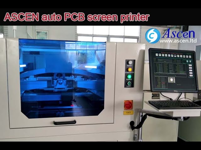
https://www.ascen.ltd/Products/Solder_paste_printer/513.html full auto PCB screen printer and SMT solder paste printing machine with Image and optical system,It is a very accurate fully automatic SMT stencil printer.automatic PCB screen printer main
Training Courses | | | IPC-6012 Specialist (CIS)
The Certified IPC-6012 Specialist (CIS) training covers design, fabrication and inspection of rigid printed boards.
Training Courses | | | Other Courses
Other courses related to electronics manufacturing and assembly
Events Calendar | Mon Apr 23 00:00:00 EDT 2018 - Thu Apr 26 00:00:00 EDT 2018 | Shanghai, China
SMTA China East Conference 2018
Events Calendar | Tue Apr 13 00:00:00 EDT 2021 - Tue Apr 13 00:00:00 EDT 2021 | ,
Boston Chapter Webinar: Cleaning Chemistry For PWB and Rework - Part 2, session 1
Career Center | Lumberton, USA | Engineering,Production
Metal Etching Technology Inc. is one of the United States leading Manufacturers of solder paste stencils for the electronics industry. Candidate's responsibilities will include printing and manipulating cad data, transferring files via internet/em
Career Center | Colorado Springs, Colorado USA | Sales/Marketing
Active customer service support for existing accounts to include both phone and email contact. Coordinate and assist with resolution of locally initialed customer concerns, complaints and corrective actions. Maintain accurate and complete territory a
Career Center | , | Engineering,Production,Quality Control
SMT EXPERT WITH DOE ,DFM AND LEAN SKILLS
Career Center | Alta Loma, California | Engineering,Quality Control,Research and Development
Rigid and Flexible Printed Circuits Plating and Metal Finishing Operations Six Sigma Work Instruction Documentation Process Development Equipment Selection and Specification New Facility Startup Air, Water and Hazardous Waste Environmental Reporting
SMTnet Express, June 27, 2019, Subscribers: 32,092, Companies: 10,819, Users: 24,882 Advanced Cu Electroplating Process for Any Layer Via Fill Applications with Thin Surface Copper Credits: MacDermid Inc. Copper-filled micro-vias are a key
SMTnet Express, March 3, 2016, Subscribers: 24,124, Companies: 15,000, Users: 40,059 Nanocopper Based Paste for Solid Copper Via Fill David Ciufo, Sujatha Ramanujan, Janet Heyen, Michael Carmody; Intrinsiq Materials , Sunny Patel; Candor
| https://pcbasupplies.com/stencil-rolls/
» Stencil Rolls Stencil Rolls Keep stencil apertures clear of paste residue during the automatic screen-printing process. DEK EKRA GKG/Juki MPM Yamaha 2 Stencil Rolls items sorted by
| http://etasmt.com/cc?ID=te_news_industry,23962&url=_print
. Is the layout designed for the PIP process? If the PCB hole diameter is too big, it will require too much solder to fill it up. If it is too small, it is very difficult to fill the hole properly with paste during solder paste printing


