Industry Directory | Manufacturer
1-20 layers PCB manufacturer, focusing on metal core pcb, multi-layer PCB, fast PCB and middle-small batch PCB. Min. circuit width & spacing: 3mil. UL, ISO9001, ROHS,ISO14001 certified.
Industry Directory | Manufacturer
professional manufacturer of pcb
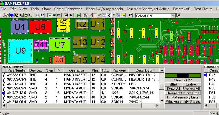
If you have only Gerber data files to work with then ProntoGERBER-CONNECTION can help you! ProntoGERBER-CONNECTION imports raw Gerber data and allows the user to add intelligent information to the shapes on the display and create process assembly

The PCB Footprint Expert is a powerful CAD library development tool powered by our own proprietary CAD LEAP Technology (Libraries Enhanced with Automated Preferences). It is packed with very powerful advanced library management features that cuts foo
Electronics Forum | Mon Jan 11 14:48:44 EST 2010 | davef
SR1000 is commonly used for tenting. Search the fine SMTnet Archives on : tenting Someone gave us this note. We have lost their name. It seems to be good advice. If Liquid Photo Image (LPI) solder mask is required, do not tent via holes. Tenting
Electronics Forum | Wed Oct 06 04:23:09 EDT 1999 | Brian
| | I am a new employee at a company that has had a large turnover of employees over the past year. I am working on a board (components on one side only), the engineer (he is also new ) wants to use an .035 pad with a .021 dia. hole, there are no via
Industry News | 2018-10-18 08:29:16.0
How to Prevent Short Circuits to Ground in QFN Components?
Industry News | 2018-12-08 03:29:29.0
SMT Dictionary – Surface Mount Technology Acronym and Abbreviation
Parts & Supplies | Circuit Board Assembly Products
1). 100mm x 98mm/1up, FR-4, 2). 1mm +/-0.1mm,6 Layers 3). 1oz copper finished 3). Green solder mask/white legend 4). Min. hole 0.15mm, 4/4 mil track/gap 5). Blind via layer 1-2, via-in-pad. 6). Immersion gold surface finish
Technical Library | 2019-06-26 23:21:49.0
Copper-filled micro-vias are a key technology in high density interconnect (HDI) designs that have enabled increasing miniaturization and densification of printed circuit boards for the next generation of electronic products. Compared with standard plated through holes (PTHs) copper filled vias provide greater design flexibility, improved signal performance, and can potentially help reduce layer count, thus reducing cost. Considering these advantages, there are strong incentives to optimize the via filling process. This paper presents an innovative DC acid copper via fill formulation, for VCP (Vertical Continues Plating) applications which rapidly fills vias while minimizing surface plating.
Technical Library | 2019-07-17 17:56:34.0
The increased demand for electronic devices in recent years has led to an extensive research in the field to meet the requirements of the industry. Electrolytic copper has been an important technology in the fabrication of PCBs and semiconductors. Aqueous sulfuric acid baths are explored for filling or building up with copper structures like blind micro vias (BMV), trenches, through holes (TH), and pillar bumps. As circuit miniaturization continues, developing a process that simultaneously fills vias and plates TH with various sizes and aspect ratios, while minimizing the surface copper thickness is critical. Filling BMV and plating TH at the same time, presents great difficulties for the PCB manufactures. The conventional copper plating processes that provide good via fill and leveling of the deposit tend to worsen the throwing power (TP) of the electroplating bath. TP is defined as the ratio of the deposit copper thickness in the center of the through hole to its thickness at the surface. In this paper an optimization of recently developed innovative, one step acid copper plating technology for filling vias with a minimal surface thickness and plating through holes is presented.
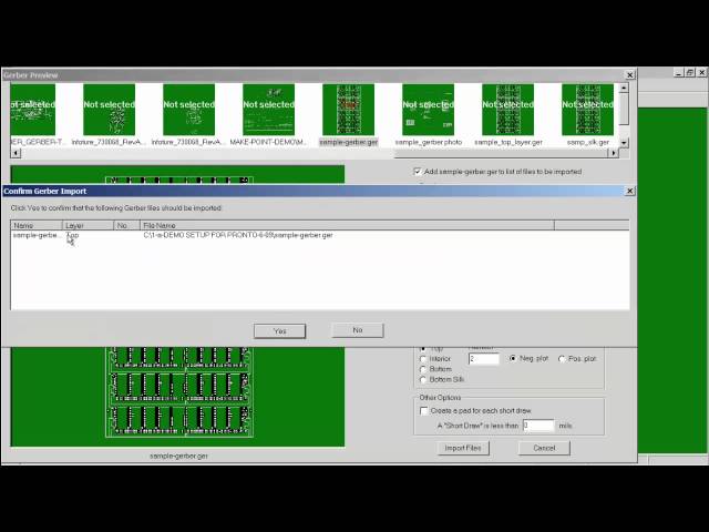
ProntoGERBER-CONNECTION software is used by electronic manufacturer & imports raw Gerber data & allows the user to add intelligent information to the shapes on the display and creates real reference designators, theta rotation, part numbers, X/Y comp
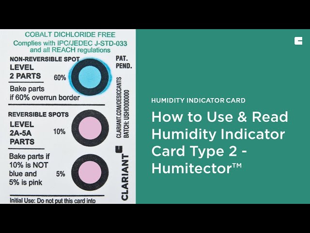
A Sustainable Alternative - Humitector cards are halogen-free and cobalt dichloride free. Visit https://www.clariant.com/solutions/products/2017/10/31/00/12/humitector-type-2-nonreversible-humidity-indicator-card?utm_source=CLRYouTube&utm_medium=Vi
Training Courses | | | IPC-6012 Specialist (CIS)
The Certified IPC-6012 Specialist (CIS) training covers design, fabrication and inspection of rigid printed boards.
Training Courses | ON DEMAND | | IPC-600 Trainer (CIT)
The Certified IPC-600 Trainer (CIT) courses recognize individuals as qualified trainers in the area of quality assurance of bare printed circuit boards and prepare them to deliver Certified IPC-600 (CIS) training.
SMT Express, Volume 2, Issue No. 3 - from SMTnet.com Volume 2, Issue No. 3 Thursday, March 16, 2000 Featured Article Return to Front Page Stencil Design for Mixed Technology Through-hole / SMT Placement and Reflow by William E. Coleman, Photo
Imagineering, Inc. | https://www.pcbnet.com/capabilities/assembly/technology-roadmap/
(HDI) Finish Hole Size • Mechanical Drill - 4 mil (HDI) • Laser Drill - 2.5 mil (HDI) True Hole Position +/-.0015" Finish Hole Size Tolerance • PTH - +/-.0015" • Non-PTH - +/-.001" Aspect Ratio (Board Tks./FHS) 30 Heavy Copper
| https://www.eptac.com/wp-content/uploads/2021/10/EPTAC_DataSheet_IPCDesigner_CID.pdf
electrical test, thermal stress, panelization, laminate selection, scoring and routing parameters, board thickness tolerance, nonfunctional lands, hole aspect ratios, via hole size and printed board


winsouce.jpg)