Industry Directory | Manufacturer
professional manufacturer of pcb
Industry Directory | Manufacturer
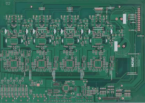
1-20 layers PCB manufacturer, focusing on metal core pcb, multi-layer PCB, fast PCB and middle-small batch PCB. Min. circuit width & spacing: 3mil. UL, ISO9001, ROHS,ISO14001 certified.
New Equipment | Education/Training
This specification covers qualification and performance of rigid PCBs including with or without plated-through holes, single-sided, double-sided, multilayer with or without blind/buried vias and metal core boards. It addresses final finish and surfac
New Equipment | Education/Training
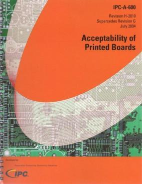
IPC A-600H Acceptability of Electronic Assemblies. The IPC-A-600, "Acceptability of Printed Boards " is the most widely used published specification on printed wiring boards. This specification has set the standard for rigid printed boards in terms o
Electronics Forum | Thu Oct 30 23:39:10 EDT 2014 | beilimanu
No paper thing, while I can make some suggestions based on my experience. what is the size of your via? If it's smaller than dia0.4mm, in PCB production process it should be filled by soldermask. So my suggestion is design it to be full filled by SM
Electronics Forum | Thu Jan 06 06:15:49 EST 2005 | mattkehoe
We need some opinions about a situation that is causing problems in our process. The pcb's in question are .125 thick with a HASL finish. The boards are coming in with a large amount of solder trapped inside the via holes. Sometimes this solder is ac
Industry News | 2010-04-10 02:09:54.0
If a picture is worth a thousand words, the new H revision of IPC-A-600, Acceptability of Printed Boards, is a priceless work of art for fabricators and assemblers, particularly inspectors and product developers. IPC — Association Connecting Electronics Industries® announces the new releases of IPC-A-600H and its companion document the C revision of IPC-6012, Qualification and Performance Specification for Rigid Printed Boards.
Industry News | 2012-04-27 19:15:46.0
Caledon Controls Ltd. has through a collaborative effort between them, Vast Films and Triangle Labs created the worlds least expensive interconnect structure (PCB).
Technical Library | 2019-07-17 17:56:34.0
The increased demand for electronic devices in recent years has led to an extensive research in the field to meet the requirements of the industry. Electrolytic copper has been an important technology in the fabrication of PCBs and semiconductors. Aqueous sulfuric acid baths are explored for filling or building up with copper structures like blind micro vias (BMV), trenches, through holes (TH), and pillar bumps. As circuit miniaturization continues, developing a process that simultaneously fills vias and plates TH with various sizes and aspect ratios, while minimizing the surface copper thickness is critical. Filling BMV and plating TH at the same time, presents great difficulties for the PCB manufactures. The conventional copper plating processes that provide good via fill and leveling of the deposit tend to worsen the throwing power (TP) of the electroplating bath. TP is defined as the ratio of the deposit copper thickness in the center of the through hole to its thickness at the surface. In this paper an optimization of recently developed innovative, one step acid copper plating technology for filling vias with a minimal surface thickness and plating through holes is presented.
Technical Library | 2019-06-06 00:19:02.0
More and more people and things are using electronic devices to communicate. Subsequently, many electronic products, in particular mobile base stations and core network nodes, need to handle enormous amounts of data per second. One important link in this communication chain is high speed pressfit connectors that are often used to connect mother boards and back planes in core network nodes. These new high speed pressfit connectors have several hundreds of thin, short and weak pins that are prone to damage. Small variations in via hole dimensions or hole plating thickness affect the connections; if the holes are too small, the pins may be bentor permanently deformed and if the holes are too large they will not form gas tight connections.The goal of this project was to understand how rework of these new high speed pressfit connectors affects connection strengths, hole wall deformations and plating cracks.

This video describes the IPC A-600 training and certification program. The IPC A-600 specification is a set of acceptability specifications for printed circuit boards. These standards determine the acceptance and reject criteria for printed wiring bo
With the development of miniaturization of assembly components, the layout area and pattern design area of PCBs have also been continuously reduced, and PCB manufacturers are constantly updating the production process to conform to the development tr
Training Courses | | | IPC-6012 Specialist (CIS)
The Certified IPC-6012 Specialist (CIS) training covers design, fabrication and inspection of rigid printed boards.
Training Courses | ON DEMAND | | IPC-600 Trainer (CIT)
The Certified IPC-600 Trainer (CIT) courses recognize individuals as qualified trainers in the area of quality assurance of bare printed circuit boards and prepare them to deliver Certified IPC-600 (CIS) training.
SMT Express, Volume 2, Issue No. 3 - from SMTnet.com Volume 2, Issue No. 3 Thursday, March 16, 2000 Featured Article Return to Front Page Stencil Design for Mixed Technology Through-hole / SMT Placement and Reflow by William E. Coleman, Photo
ATTENDANT WET CHEMICAL PROCESSES) Hole wall preparatio
PCB Libraries, Inc. | https://www.pcblibraries.com/forum/RSS_pcb-design-basics_forum8.xml
: smallest via hole that can use a +/- 3 mils Author: Tom HSubject: smallest via hole that can use a +/- 3 milsPosted: 17 Jun 2019 at 11:26am0.20 mm (8 mils) However, there are high quality fabrication shops that say they can do
| https://www.eptac.com/wp-content/uploads/2021/11/webinar_eptac_04_16_08.pdf


winsouce.jpg)