Industry Directory | Manufacturer
UWELLPCB.com is the PCB supplier. We offer PCB from single side board, double side PCB to 32layer board,including the Rigid PCB, Flex PCB, Rigid-flex PCB,Quick-turn prototype and PCB assembly
Industry Directory | Manufacturer
PCBCart, a highly skilled PCB Fab, Parts Sourcing & Assembly services provider for global companies, fabricates 23k+ different PCB designs each year, and are committed on the quality & performance of every circuit board it printed
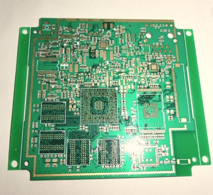
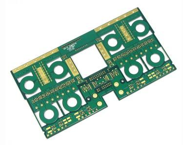
Layer: 6 layers Material: FR-4 Board Thickness: 1.0mm Surface Finish:ENIG Copper Thickness: 1 oz all layers Blind via L1~L2 and L1~L3 Layers: 2--36layers Max manufacturing size: 640mm*1100mm Copper foil thickness: 0.5OZ-13OZ Min line width
New Equipment | Design Services
Layer:4 Material:FR-4 4/4/4/4oz Thickness:2.0 Minimum hole:0.35mm Minimum Tracc/Spacing:12mil/15mil Application:power supply Layers: 2--36layers Max manufacturing size: 640mm*1100mm Copper foil thickness: 0.5OZ-13OZ Min line width/space:
Electronics Forum | Thu Jan 06 08:03:47 EST 2005 | davef
On solder in vias: It looks like the via are not solder masked well and pick-up solder either: * Solder coating ... OR * During leveling It's possible that the design specifies openings in the solder mask for these via. On solder in the unsupporte
Electronics Forum | Tue Jul 06 18:16:14 EDT 1999 | Boca
| | Is anyone aware of some guidelines regarding through-hole in SMT pads? One of our designers wants to add through-hole leads in some SMT pads for an inductor. The size of the hole is 0.032 inches and takes-up approximately 25% of the pad area.
Industry News | 2017-04-11 21:19:32.0
GPD Global offers versatile large format inline dispensing systems and stand-alone liquid dispense technologies for maximizing product yield. This is the largest standard PCB dispensing system platform in the industry.
Industry News | 2012-04-06 15:32:39.0
GPD Global, a manufacturer of precision fluid dispensing systems for high-volume 24/7, low-volume/high-mix and R&D production, announces the global release of its PCD4 Dispense Pump after its successful release and testing in the North American market.
.jpg)
Parts & Supplies | SMT Equipment
Panasonic smt nozzles models: Panasonic MSR SMT NOZZLE Part Number Description 10468S0002 MSR - SMT NOZZLE - VVS (0.84 X 0.60) 10468S0003 - NZ. - VS (1.0 X 0.64) 10468S0004 -NZ. - S (1.6 X 1.06) 1046710134 -NZ. - M (1.60mm) 10467S0001 -NZ. - L
Parts & Supplies | SMT Equipment
Panasonic smt nozzles models: Panasonic MSR SMT NOZZLE Part Number Description 10468S0002 MSR - SMT NOZZLE - VVS (0.84 X 0.60) 10468S0003 - NZ. - VS (1.0 X 0.64) 10468S0004 -NZ. - S (1.6 X 1.06) 1046710134 -NZ. - M (1.60mm) 10467S0001 -NZ. - L
Technical Library | 2019-10-10 00:26:28.0
Voids are a plague to our electronics and must be eliminated! Over the last few years we have studied voiding in solder joints and published three technical papers on methods to "Fill the Void." This paper is part four of this series. The focus of this work is to mitigate voids for via in pad circuit board designs. Via holes in Quad Flat No-Lead (QFN) thermal pads create voiding issues. Gasses can come out of via holes and rise into the solder joint creating voids. Solder can also flow down into the via holes creating gaps in the solder joint. One method of preventing this is via plugging. Via holes can be plugged, capped, or left open. These via plugging options were compared and contrasted to each other with respect to voiding. Another method of minimizing voiding is through solder paste stencil design. Solder paste can be printed around the via holes with gas escape routes. This prevents gasses from via holes from being trapped in the solder joint. Several stencil designs were tested and voiding performance compared and contrasted. In many cases voiding will be reduced only if a combination of mitigation strategies are used. Recommendations for combinations of via hole plugging and stencil design are given. The aim of this paper is to help the reader to "Fill the Void."
Technical Library | 2020-07-15 18:49:03.0
Via Filling • Through Hole Vias - IPC-4761 – Plugging – Filling – Filled & Capped • MicroviaFilling and Stacked Vias

The PCB Footprint Expert is a powerful CAD library development tool powered by our own proprietary CAD LEAP Technology (Libraries Enhanced with Automated Preferences). It is packed with very powerful advanced library management features that cuts foo

Teaching video on PCB through hole repair. BEST instructors teach the method for repair of a damaged eyelet using a multitude of different close up and angled views. Repair is completed per the IPC 7721 instructions. http://www.solder.net
Training Courses | | | PCB Assembly Courses
The PCB assembly courses provide knowledge of different processes and equipment used in TH and SMT assembly of printed circuit boards.
SMT Express, Volume 2, Issue No. 3 - from SMTnet.com Volume 2, Issue No. 3 Thursday, March 16, 2000 Featured Article Return to Front Page Stencil Design for Mixed Technology Through-hole / SMT Placement and Reflow by William E. Coleman, Photo
| https://pcbasupplies.com/ezload-replacment-pads/
? Please enter your username or email address. You will receive a link to create a new password via email. Email Reset Link Shopping cart 0 There are no products in the cart!
| https://www.eptac.com/soldertips/soldertips-issues-with-incomplete-solder-reflow-in-production-2/
SolderTips: Issues With Incomplete Solder Reflow in Production | EPTAC Skip to content Scroll Toll Free: 800.643.7822 Toggle navigation Training All Classes


