Industry Directory | Manufacturer
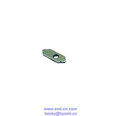
Our wide-ranging product include conventional FR-4, High TG FR-4, High-density with blind and buried vias, thick copper,thick gold plating, High frequency, FPC board, Rigid-flex PCB, Meta Core PCB ect
Industry Directory | Manufacturer
professional manufacturer of pcb
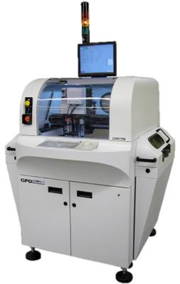
Precision Dispensing System for Heated Dispense Applications The GPD Global MAX II is a compact; high-accuracy system designed for today’s advanced heated dispensing applications. The frame is molded from “liquid rock” which gives the system a stabl
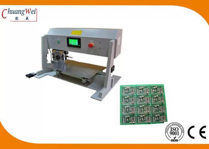
Pre-scored Automatic PCB Depaneling Machine with Large LCD Display Specification: Power :AC 110 / 220 V 50 / 60HZ Dimension :780 × 400 × 450mm Blade Route :430mm / Max Blade Speed :500mm / sec Down- Blade Size :500 mm Cutting length :460mm Mac
Electronics Forum | Mon Feb 26 20:02:42 EST 2001 | davef
First, I don�t understand why your board fabricator can�t do a good job plugging your vias. Additionally, when you consider that they forgot to plug the first batch of boards, it makes me wonder if they are desirable as a supplier. Generally, we us
Electronics Forum | Thu Oct 07 20:34:48 EDT 1999 | Tony Huang
Hi, Does anybody know what is the minimum gold plating thickness on the PCB goldfinger required by the industrial specifications - IPC, Bellcore, etc. Where can I find the information? Appreciate for the help! Thanks, Tony
Used SMT Equipment | Screen Printers
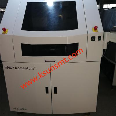
MPM Momentum+ Printer Substrate treatment Maximum plate size(XxY) 609.6 mm x 508 mm(24”x 20”) Segmented mode-Momentum Elite 457 mm x 508 mm(18"x20") Minimum Plate Size (XxY)
Used SMT Equipment | Screen Printers
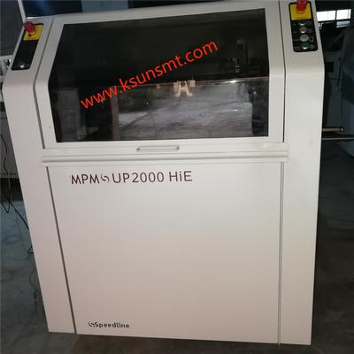
MPM UP2000HiE PRINTER Substrate treatment Minimum/maximum size 2"x 2"(50.0 mm x50.0 mm) to 20" x 16" (508 mm x 406 mm)(16 "or larger substrate requires special clamps) Thickness rang
Industry News | 2003-05-19 10:06:43.0
The PCB is available with a maximum panel size of 406-by-460mm and a minimum board thickness of 0.8mm.
Industry News | 2003-02-25 08:18:29.0
Teradyne can now provide deep micro-via technology for customers of high-performance printed circuits.
_1.JPG)
Parts & Supplies | Pick and Place/Feeders
KGA-M880C-10 REEL CERAMIC 1005 YAMAHA SS ZS Electric feeder X-direction Adjusting Gasket, 8MM-104MM KHJ-MC107-00 thickness 0.01MM KHJ-MC10V-00 thickness 0.02MM KHJ-MC10U-00 thickness 0.03MM KHJ-MC108-00 thickness 0.05MM KHJ-MC10G-00 thickness 0
Parts & Supplies | Pick and Place/Feeders
Fuji NXT pressure material cover shrapnel PP03342 PP03341 steel plate with hook PJ00143 FUJI NXT scrap with guide wheel ROLLER PJ00162 FUJI NXT scrap with gear (thick) PJ00172 FUJI NXT scrap with gear (thin) PJ02960 FUJI NXT 2 grid switch PJ038
Technical Library | 2020-07-22 19:39:05.0
The PWB industry needs to complete reliability testing in order to define the minimum copper wrap plating thickness requirement for confirming the reliability of PTH structures. Predicting reliability must ensure that the failure mechanism is demonstrated as a wear-out failure mode because a plating wrap failure is unpredictable. The purpose of this study was to quantify the effects of various copper wrap plating thicknesses through IST testing followed by micro sectioning to determine the failure mechanism and identify the minimum copper wrap thickness required for a reliable PWB. Minimum copper wrap plating thickness has become an even a bigger concern since designers started designing HDI products with buried vias, microvias and through filled vias all in one design. PWBs go through multiple plating cycles requiring planarization after each plating cycle to keep the surface copper to a manageable thickness for etching. The companies started a project to study the relationship between Copper wrap plating thickness and via reliability. The project had two phases. This paper will present findings from both Phase 1 and Phase 2.
Technical Library | 2019-07-17 17:56:34.0
The increased demand for electronic devices in recent years has led to an extensive research in the field to meet the requirements of the industry. Electrolytic copper has been an important technology in the fabrication of PCBs and semiconductors. Aqueous sulfuric acid baths are explored for filling or building up with copper structures like blind micro vias (BMV), trenches, through holes (TH), and pillar bumps. As circuit miniaturization continues, developing a process that simultaneously fills vias and plates TH with various sizes and aspect ratios, while minimizing the surface copper thickness is critical. Filling BMV and plating TH at the same time, presents great difficulties for the PCB manufactures. The conventional copper plating processes that provide good via fill and leveling of the deposit tend to worsen the throwing power (TP) of the electroplating bath. TP is defined as the ratio of the deposit copper thickness in the center of the through hole to its thickness at the surface. In this paper an optimization of recently developed innovative, one step acid copper plating technology for filling vias with a minimal surface thickness and plating through holes is presented.
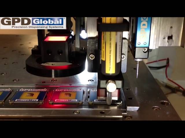
Precision Dispensing System for Heated Dispense Applications The GPD Global MAX II is a compact; high-accuracy system designed for today’s advanced heated dispensing applications. The frame is molded from “liquid rock” which gives the system a stabl
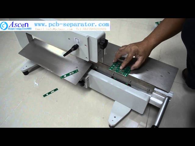
http://www.pcb-separator.com/ https://www.pcb-separator.com/html/PRODUCTS/PCB%20separator/2019/1113/832.html Hand push pcb cutter/PCB cutting machine manufacturer/PCB V-cut machine manufacturer/PCB depaneling equipment, automatic pcb cutting machine,
Training Courses | | | IPC-6012 Specialist (CIS)
The Certified IPC-6012 Specialist (CIS) training covers design, fabrication and inspection of rigid printed boards.
Training Courses | | | IPC-6012 Trainer (CIT)
The Certified IPC-6012 Trainer (CIT) courses recognize individuals as qualified trainers in the area of design, fabrication and inspection of rigid printed boards and prepare them to deliver Certified IPC-6012 Specialist (CIS) training.
Events Calendar | Mon Sep 14 00:00:00 EDT 2020 - Mon Sep 14 00:00:00 EDT 2020 | ,
Printed Circuit Board (PCB) Inspection & Quality Control
Events Calendar | Wed Jul 03 00:00:00 EDT 2024 - Wed Jul 03 00:00:00 EDT 2024 | ,
Europe Chapter Webinar: "Back-to-Basics" SMT Assembly
Career Center | Dana Point, California USA | Sales/Marketing
We are currently seeking sales reps nationwide for this rapidly growing supplier of printed circuit boards (since 1986)with facilities in southern CA and eight PCB facilities in China and Taiwan, all ISO 9002 certified and UL94V-0 approved, some are
Career Center | , | Engineering,Research and Development,Technical Support
INTRODUCTION Ref: TR/EMP/EXP/VOL.IV/05 Mobil Consulting/Recruiting Services; Pursuant to the service contract with the NIGERIAN MOBIL OIL COMPANY (NMOC) FIELD DEVELOPMENT PROJECT in Nigeria, has been mandated to recruit senior services expatriat
Career Center | Erode, Tamilnadu India | Engineering
Professional Summary 3+ years of experience in the PCB CAM engineering Exposure to FRONTLINE GENESIS 2000 Having exposure in UCAM Exposure to Create, Array & Panelize it for manufacturability Experienced in Creating impedance cou
Career Center | Shen Zhen, China | Management,Sales/Marketing
Working in GLORYPCB for 10 years.knowing electronic supply chain very well. especially for PCB PCBA assembly and other Electronic Manufacturing Service.Glorypcb is a professional electronic manufacturer located in Shenzhen with three facilities.offe
SMTnet Express, July 18, 2019, Subscribers: 32,162, Companies: 10,836, Users: 24,951 Via Fill and Through Hole Plating Process with Enhanced TH Microdistribution Credits: MacDermid Inc. The increased demand for electronic devices in recent years
ASYMTEK Products | Nordson Electronics Solutions | https://www.nordson.com/en/divisions/asymtek/your-process/video-library/emi-conductive-coating-solution-achieving-a-target-thickness-of-25-um
EMI Conductive Coating Solution - Achieving a Target Thickness of 25 µm | Nordson ASYMTEK ASYMTEK Products Corporate | Global Directory | Languages Division Only All of Nordson Fluid Dispensing Systems Jets
| http://etasmt.com/cc?ID=te_news_industry,24564&url=_print
. The plating thickness is too thin or the result of poor processing, which can be easily damaged during assembly; The soldering temperature is not high enough


