Industry Directory | Manufacturer
Manufacturer of flex, rigid-flex, and rigid circuit boards. We offer prototype and production delivery options. We manufacture commercial, military, medical and industrial jobs and offer value added services such as assembly. We can customize services to fit your needs, such as gold or white tin plating, plugged or blind vias, etc.
Industry Directory | Manufacturer
PCB Repairs of all kinds including-Solder on Tab (Solder Removal, Gold Plating), PTH & Delam repairs, etc.
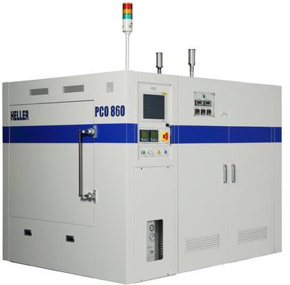
New Equipment | Curing Equipment
A Pressure Cure Oven (PCO), or Autoclave, is used to minimize voiding and increase adhesion strength for bonding processes typically used in die attach and underfill applications. PCO pressurizes air into a rigid vessel and heats & cools with
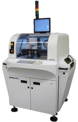
Precision Dispensing System for Heated Dispense Applications The GPD Global MAX II is a compact; high-accuracy system designed for today’s advanced heated dispensing applications. The frame is molded from “liquid rock” which gives the system a stabl
Electronics Forum | Fri Aug 16 10:00:03 EDT 2002 | davef
You have a very bad situation. It�s tough for the gas, flux material, er whatever to escape when the BGA is sitting on top of it and the blind via is blocking it from the other side. Obviously the vias should have been: * Placed on the edge of the
Electronics Forum | Mon Sep 30 09:26:04 EDT 2002 | itempea
Russ, first step would be to get IPC-7095 on BGAs. A few notes: There can be voids in solder balls, or at the solder joints to the BGA, or at the solder joints to the PCB. Various sources or reasons can be responsible for these voids. Voids can be
Industry News | 2018-10-18 10:40:04.0
Via Tent-Holes with Solder Mask
Industry News | 2018-08-16 19:58:50.0
The SMTA Capital Chapter is holding its upcoming Capital Expo and Tech Forum at Johns Hopkins University / Applied Physics Lab, Kossiakoff Center, 11100 Johns Hopkins Road, Laurel, MD 20723, on Thursday, August 23rd.

Parts & Supplies | Circuit Board Assembly Products
1). 80 *190mm/2up, FR-4 2). 6 layers at 1.4mm thick 3). 35 μm copper weight 4). Green solder mask LPI/White legend 5). ENIG surface finish 6). Blind via from Layer 1 to layer 2 7). Via in pad plugged conductive resin
Technical Library | 2019-10-10 00:26:28.0
Voids are a plague to our electronics and must be eliminated! Over the last few years we have studied voiding in solder joints and published three technical papers on methods to "Fill the Void." This paper is part four of this series. The focus of this work is to mitigate voids for via in pad circuit board designs. Via holes in Quad Flat No-Lead (QFN) thermal pads create voiding issues. Gasses can come out of via holes and rise into the solder joint creating voids. Solder can also flow down into the via holes creating gaps in the solder joint. One method of preventing this is via plugging. Via holes can be plugged, capped, or left open. These via plugging options were compared and contrasted to each other with respect to voiding. Another method of minimizing voiding is through solder paste stencil design. Solder paste can be printed around the via holes with gas escape routes. This prevents gasses from via holes from being trapped in the solder joint. Several stencil designs were tested and voiding performance compared and contrasted. In many cases voiding will be reduced only if a combination of mitigation strategies are used. Recommendations for combinations of via hole plugging and stencil design are given. The aim of this paper is to help the reader to "Fill the Void."
Technical Library | 2020-07-15 18:49:03.0
Via Filling • Through Hole Vias - IPC-4761 – Plugging – Filling – Filled & Capped • MicroviaFilling and Stacked Vias
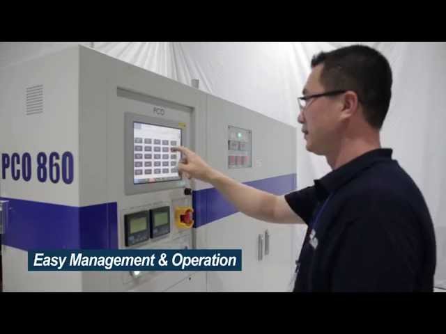
General curing, die attach curing, underfill curing, film & tape bonding, wafer laminating.
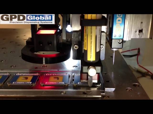
Precision Dispensing System for Heated Dispense Applications The GPD Global MAX II is a compact; high-accuracy system designed for today’s advanced heated dispensing applications. The frame is molded from “liquid rock” which gives the system a stabl
Training Courses | | | IPC-6012 Specialist (CIS)
The Certified IPC-6012 Specialist (CIS) training covers design, fabrication and inspection of rigid printed boards.
Training Courses | | | PCB Assembly Courses
The PCB assembly courses provide knowledge of different processes and equipment used in TH and SMT assembly of printed circuit boards.
Events Calendar | Thu Oct 03 00:00:00 EDT 2019 - Thu Oct 03 00:00:00 EDT 2019 | ,
IPC Tech Ed Webinar Series: Ball Grid Array (BGA) and Bottom Termination Component (BTC) Design and Assembly Challenges: Reflow Profiling to Achieve Low Defect Rates and Successful Assembly! – Part 2
Events Calendar | Mon Apr 23 00:00:00 EDT 2018 - Thu Apr 26 00:00:00 EDT 2018 | Shanghai, China
SMTA China East Conference 2018
SMTnet Express, October 10, 2019, Subscribers: 32,263, Companies: 10,893, Users: 25,93 Fill the Void IV: Elimination of Inter-Via Voiding Credits: FCT ASSEMBLY, INC. Voids are a plague to our electronics and must be eliminated! Over the last few
SMTnet Express, July 16, 2020, Subscribers: 28,512, Companies: 11,045, Users: 25,964 Via In Pad - Conductive Fill or Non-Conductive Fill? Credits: Advanced Circuits In the early 2000s the first fine-pitch ball grid array devices became popular
PCB Libraries, Inc. | https://www.pcblibraries.com/forum/RSS_pcb-via-terms-and-applications_topic1596.xml
) is covered with solder mask. Mask Plugged Via: for this specific measures are taken to ensure the via is plugged and sealed with mask and the annular ring is covered


