New Equipment | Soldering - Other
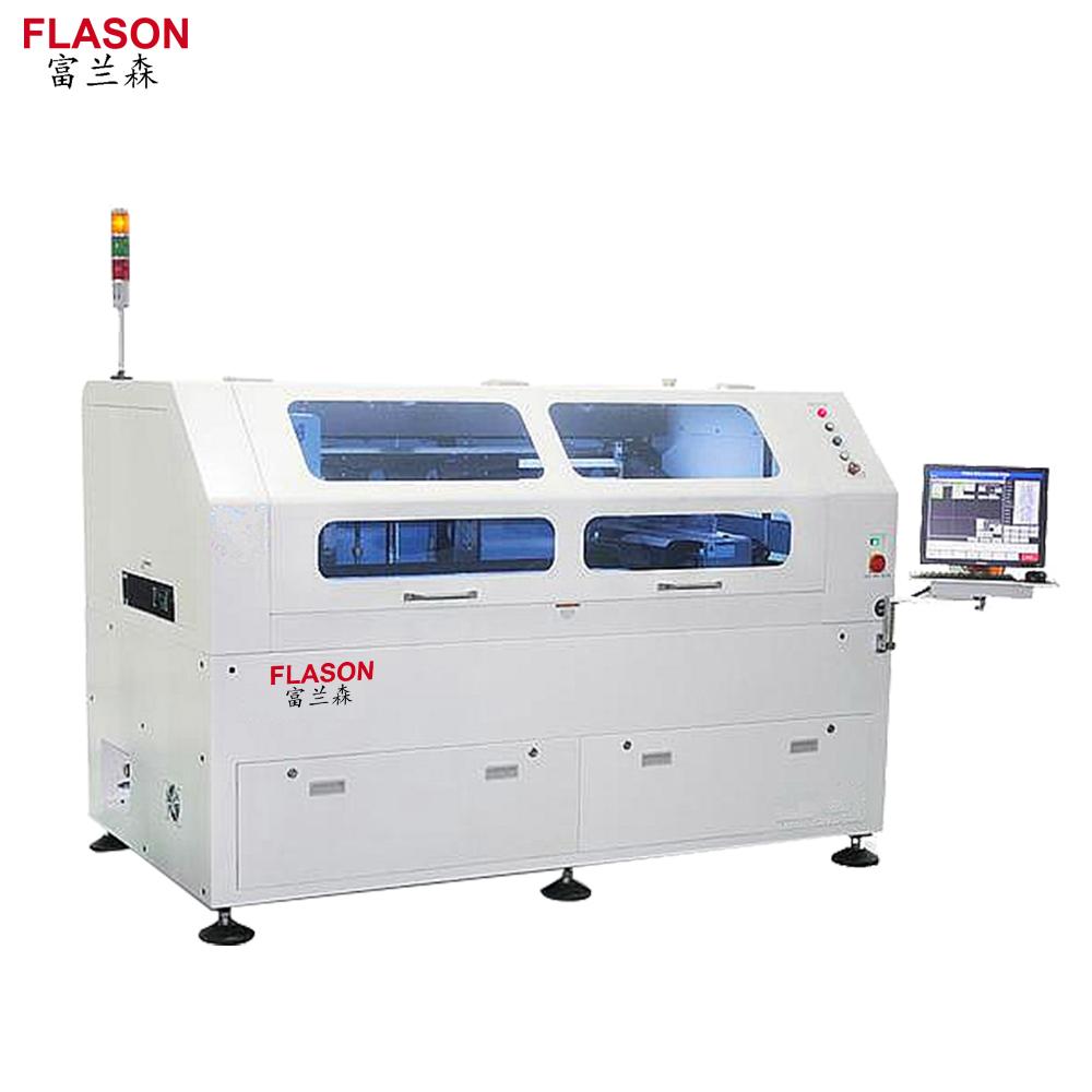
SMT Stencil Printer Automatic 1200mm Solder paste printer for SMT assembly line Power Supply: AC:220±10%,50/60HZ Control Method: PC Control PCB Size/Max:1200*340mm Weight Approx:1500Kg Product description: Automatic1200mm So
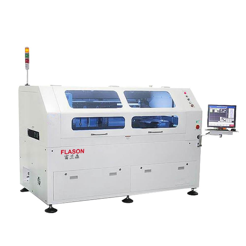
Flason SMT Automatic SMT 1200mm Solder paste printer for SMT assembly line Power Supply: AC:220±10%,50/60HZ Control Method: PC Control PCB Size/Max:1200*340mm Weight Approx:1500Kg Product description: Automatic1200mm SMT Solder paste p
Industry News | 2018-10-18 11:19:07.0
How To Design Cost-Effective PCBs
Technical Library | 2019-08-07 22:56:45.0
The requirement to reconsider traditional soldering methods is becoming more relevant as the demand for bottom terminated components (QFN/BTC) increases. Thermal pads under said components are designed to enhance the thermal and electrical performance of the component and ultimately allow the component to run more efficiently. Additionally, low voiding is important in decreasing the current path of the circuit to maximize high speed and RF performances. The demand to develop smaller, more reliable, packages has seen voiding requirements decrease below 15 percent and in some instances, below 10 percent.Earlier work has demonstrated the use of micro-fluxed solder preforms as a mechanism to reduce voiding. The current work builds upon these results to focus on developing an engineered approach to void reduction in leadless components (QFN) through increasing understanding of how processing parameters and a use of custom designed micro-fluxed preforms interact. Leveraging the use of a micro-fluxed solder preform in conjunction with low voiding solder paste, stencil design, and application knowhow are critical factors in determining voiding in QFN packages. The study presented seeks to understand the vectors that can contribute to voiding such as PCB pad finish, reflow profile, reflow atmosphere, via configuration, and ultimately solder design.A collaboration between three companies consisting of solder materials supplier, a power semiconductor supplier, and an electronic assembly manufacturer worked together for an in-depth study into the effectiveness of solder preforms at reducing voiding under some of the most prevalent bottom terminated components packages. The effects of factors such as thermal pad size, finish on PCB, preform types, stencil design, reflow profile and atmosphere, have been evaluated using lead-free SAC305 low voiding solder paste and micro-fluxed preforms. Design and manufacturing rules developed from this work will be discussed.

With the development of miniaturization of assembly components, the layout area and pattern design area of PCBs have also been continuously reduced, and PCB manufacturers are constantly updating the production process to conform to the development tr
| http://www.feedersupplier.com/SMT_THROUGH_HOLE
DIFFERENCES BETWEEN SMT & THROUGH-HOLE TECHNOLOGY-GOLDLAND SMT/AI Equipment & Parts wholesaler in China ---- Your best partner 简体中文 English 首页 产品展示 关于我们 联系我们 1 新闻中心 CONTACT US 新闻中心 罗女士
Imagineering, Inc. | https://www.pcbnet.com/blog/hdi-microvias-and-printed-circuit-boards/
– A hole layered between the top and bottom of a printed circuit board that connects multiple parts of a printed circuit board. Because they are not visible without a cross section of a PCB, they are also known as hidden vias


