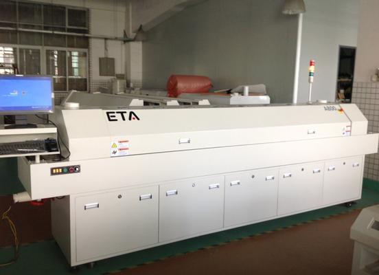
Full Hot Air Lead-Free Reflow Oven With PC Temp Control System (A800) Introduce: 1, Heating system adopts ETA patent heating technology 2, The use of imported large current solid state relay contact output, safe, reliable, equipped with a dedicated
New Equipment | Solder Materials
Indium Corporation manufactures high quality solder powders and pastes. Powders are available in hundreds of alloys and a full range of sizes. Solder pastes can be made from these powders using a wide variety of flux vehicles to get the best fit for
Electronics Forum | Thu Nov 15 08:25:08 EST 2007 | rgduval
I do think that the designer goofed, and used too large vias. I believe he only used on size via on the entire board, regardless of whether it was in a pad, or out on the board. I have seen vias in pad work, though. From a manufacturing standpoint
Electronics Forum | Tue Jul 18 13:52:42 EDT 2006 | SWAG
Could it be an unmasked via attached to the SMD pad under the part???
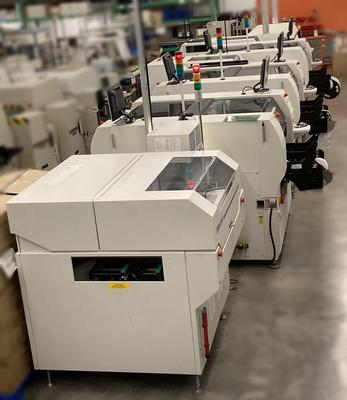
Used SMT Equipment | Turnkey Lines
Functional Pre-Owned Complete SMT Assembly Line - Still Operational (Subject to prior sell, I am listing this on other venues) Up for sale is a full turnkey SMT line and all of it's accessories, of which there are a lot, fe
Industry News | 2018-10-18 09:02:41.0
How to Solder a Surface Mount Device to a PCB Pad
Industry News | 2018-10-18 08:29:16.0
How to Prevent Short Circuits to Ground in QFN Components?
Technical Library | 2016-10-20 18:13:34.0
Pad cratering failure has emerged due to the transition from traditional SnPb to SnAgCu alloys in soldering of printed circuit assemblies. Pb-free-compatible laminate materials in the printed circuit board tend to fracture under ball grid array pads when subjected to high strain mechanical loads. In this study, two Pb-free-compatible laminates were tested, plus one dicycure non-Pb-free-compatible as control. One set of these samples were as-received and another was subjected to five reflows. It is assumed that mechanical properties of different materials have an influence on the susceptibility of laminates to fracture. However, the pad cratering phenomenon occurs at the layer of resin between the exterior copper and the first glass in the weave. Bulk mechanical properties have not been a good indicator of pad crater susceptibility. In this study, mechanical characterization of hardness and Young’s modulus was carried out in the critical area where pad cratering occurs using nano-indentation at the surface and in a cross-section. The measurements show higher modulus and hardness in the Pb-free compatible laminates than in the dicy-cured laminate. Few changes are seen after reflow – which is known to have an effect -- indicating that these properties do not provide a complete prediction. Measurements of the copper pad showed significant material property changes after reflow.
Technical Library | 2019-08-07 22:56:45.0
The requirement to reconsider traditional soldering methods is becoming more relevant as the demand for bottom terminated components (QFN/BTC) increases. Thermal pads under said components are designed to enhance the thermal and electrical performance of the component and ultimately allow the component to run more efficiently. Additionally, low voiding is important in decreasing the current path of the circuit to maximize high speed and RF performances. The demand to develop smaller, more reliable, packages has seen voiding requirements decrease below 15 percent and in some instances, below 10 percent.Earlier work has demonstrated the use of micro-fluxed solder preforms as a mechanism to reduce voiding. The current work builds upon these results to focus on developing an engineered approach to void reduction in leadless components (QFN) through increasing understanding of how processing parameters and a use of custom designed micro-fluxed preforms interact. Leveraging the use of a micro-fluxed solder preform in conjunction with low voiding solder paste, stencil design, and application knowhow are critical factors in determining voiding in QFN packages. The study presented seeks to understand the vectors that can contribute to voiding such as PCB pad finish, reflow profile, reflow atmosphere, via configuration, and ultimately solder design.A collaboration between three companies consisting of solder materials supplier, a power semiconductor supplier, and an electronic assembly manufacturer worked together for an in-depth study into the effectiveness of solder preforms at reducing voiding under some of the most prevalent bottom terminated components packages. The effects of factors such as thermal pad size, finish on PCB, preform types, stencil design, reflow profile and atmosphere, have been evaluated using lead-free SAC305 low voiding solder paste and micro-fluxed preforms. Design and manufacturing rules developed from this work will be discussed.

· What is the difference between SMT vacuum reflow soldering machine and ordinary reflow soldering machine? · What problems can be solved by smt vacuum reflow soldering machine? · What is the basic principle of vacuum reflow machine? · Ho
Full Hot Air Lead-Free Reflow Oven With PC Temp Control System (A800) Introduce: 1, Heating system adopts ETA patent heating technology 2, The use of imported large current solid state relay contact output, safe, reliable, equipped with a dedicated
Events Calendar | Mon Apr 23 00:00:00 EDT 2018 - Thu Apr 26 00:00:00 EDT 2018 | Shanghai, China
SMTA China East Conference 2018
Career Center | , | Engineering,Production,Quality Control
SMT EXPERT WITH DOE ,DFM AND LEAN SKILLS
| http://etasmt.com/cc?ID=te_news_industry,24163&url=_print
. If the cohesive force among metal powders in solder paste is smaller than the force created by the gasification, a small amount of solder paste will leave the soldering pad and some of them may hide under the chip components. When reflow soldering
| https://www.smtfactory.com/I-C-T-SMT-Vacuum-Reflow-Oven-Machine-helps-you-to-solve-the-problem-of-High-Solder-Voids-Rates-id45973467.html
also becomes an indicator of whether the product is qualified. The causes of these solder join voids are various, such as solder paste, PCB surface treatment, reflow temperature curve setting, reflow environment, solder pad design, microholes, solder pad empty, etc