Electronics Forum | Sun Mar 28 18:49:36 EDT 2021 | mekmat544
Hello, I would like to ask you if there is some formula how to calculate PTH hole and annual ring for pin in paste technology? Thank you. Mekmat.
Electronics Forum | Thu Jun 10 19:10:05 EDT 2021 | kojotssss
Hi, Get your account. https://software.indium.com/stencil-coach/pin-in-paste-apertures.php
Industry News | 2011-03-31 11:54:23.0
Over the past few years, pad cratering has become a vexing problem in lead-free assemblies, largely attributed to problems with the resin used to make a printed board. To help industry eliminate the defect and, at the same time, cut costs, IPC — Association Connecting Electronics Industries® has released IPC-9708, Test Methods for Characterization of PCB Pad Cratering.
Industry News | 2018-10-18 08:34:52.0
How to Prevent Solder Bridging in 3528 PLCC6 RGB LEDs?
Technical Library | 2019-07-24 23:55:32.0
Voiding is a key concern for components with thermal planes because interruptions in Z-axis continuity of the solder joint will hinder thermal transfer. When assembling components with solder paste, there is a high propensity for voiding due to the confined nature of the solder paste deposits under the component. Once reflowed, many factors contribute to the amount of voiding in a solder joint such as the reflow profile, designs of the component, board and stencil, and material factors. This study will focus on the solder paste alloy and flux combination as well as profile and board surface finishes.
Technical Library | 2008-03-18 12:36:31.0
This paper examines the construction of a notebook mainboard with more than 2000 components and no wave soldering required. The board contains standard SMD, chipset BGAs, connectors, through hole components and odd forms placed using full automation and soldered after two reflow cycles under critical process parameters. However, state of the art technology does not help if the process parameters are not set carefully. Can all complex BGAs, THTs and even screws be soldered on a single stencil? What will help us overcome bridging, insufficient solder and thombstoning issues? This paper will demonstrate the placement of all odd shape components using pin-in-paste stencil design and full completion of the motherboard after two reflow cycles.
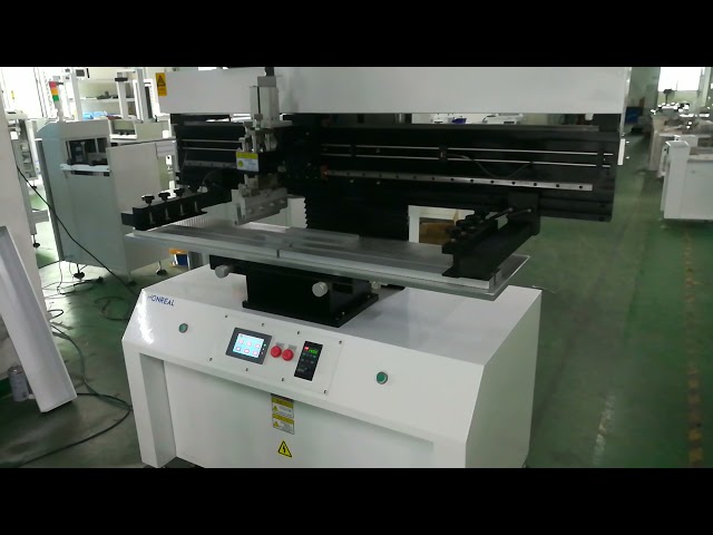
SMT Semi Auto Screen Printer for pcb size 1200 in smt LED production line Product introduction: 1.Using precision guide rail and the import motor to drive the blade seat conversion, printing, and high accuracy. 2.Printing scraper can rotate 45
Training Courses | | | PCB Assembly Courses
The PCB assembly courses provide knowledge of different processes and equipment used in TH and SMT assembly of printed circuit boards.
Events Calendar | Thu Oct 28 00:00:00 EDT 2021 - Thu Oct 28 00:00:00 EDT 2021 | ,
Juarez Chapter Webinar: Pin in Paste
SMTnet Express, April 22, 2021, Subscribers: 27,222, Companies: 11,340, Users: 26,602 Effect Of Vacuum Reflow On Solder Joint Voiding In Bumped Components Voids affect the thermal characteristics and mechanical properties of a solder
SMT Express, Volume 2, Issue No. 3 - from SMTnet.com Volume 2, Issue No. 3 Thursday, March 16, 2000 Featured Article Return to Front Page Curtailing Voids in Fine Pitch Ball Grid Array Solder Joints by Gary Morrison and Kevin Lyne
PCB Libraries, Inc. | https://www.pcblibraries.com/forum/pin-in-paste_topic3208.html
Pin in Paste - PCB Libraries Forum Forum Home > PCB Footprint Expert > Questions & Answers New Posts FAQ Search Events Register Login Pin in Paste
| http://etasmt.com/cc?ID=te_news_industry,23962&url=_print
The Application of the Pin-in-Paste Reflow Process-SMT Technical-Reflow oven,SMT Reflow Soldering Oven-cmsadmin Reflow oven,SMT Reflow Soldering Oven 当前位置: Home >> News


