
New Equipment | Soldering - Other
Sunny Company:Beijing Chengliankaida Technology Co.,Ltd Address : SanCang Road Sanjianfang airport ,Tongzhou district , Beijing China Email: salemachines@bjclkdkj.cn Skype :smdsupplier Whatsapp: +86 159 01434496 Wechat: + 86 159 0143 4496
New Equipment | Solder Materials
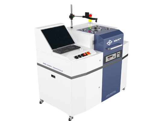
Big-Size Vacuum Soldering Oven for IGBT, MOS 1.Reflow soldering Typically high number of voids cause a large non conductive area 2.Vacuum soldering Very low number of voids, Typically 3.Applications Power Semiconductors;Hybrid
Electronics Forum | Tue Jan 14 12:20:33 EST 2020 | cyber_wolf
If you are using standard alloy and flux types and you are within the ballpark of 30-90 seconds above liquidous you should be fine. As I said above unless your profile is grossly off, it is not the cause of your voids.
Electronics Forum | Thu Jan 02 22:09:15 EST 2020 | Zack
Hello, Can you give more detail on LGA parts in question? is 50 mm x 50 mm is overall size of the parts? What about pad pitch and how big is the pads individually? I assume that 50x50 mm is overall size. How about the stencil opening for the LGA pad
Industry News | 2003-05-30 08:09:11.0
A new compact package integrates a Hall-effect sensor IC with a back-biasing magnet to achieve high airgap performance and meet restrictive space requirement.
Industry News | 2003-03-06 08:29:50.0
Coretec experienced sequential growth in sales over the last four quarters and, while its yearly sales did decline, said its sales record still compares favorably
Technical Library | 2017-11-08 23:22:04.0
Due to the ongoing trend towards miniaturization of power components, the need for increased thermal conductivity of solder joints in SMT processes gains more and more importance. Therefore, the role of void free solder joints in power electronics becomes more central. Voids developed during soldering reduce the actual thermal transfer and can cause thermal damage of the power components up to their failure. For this reason, the company has developed a new technique to minimize the formation of these voids during the soldering process.
Technical Library | 2020-11-24 23:01:04.0
The miniaturization trend is driving industry to adopting low standoff components or components in cavity. The cost reduction pressure is pushing telecommunication industry to combine assembly of components and electromagnetic shield in one single reflow process. As a result, the flux outgassing/drying is getting very difficult for devices due to poor venting channel. This resulted in insufficiently dried/burnt-off flux residue. For a properly formulated flux, the remaining flux activity posed no issue in a dried flux residue for no-clean process. However, when venting channel is blocked, not only solvents remain, but also activators could not be burnt off. The presence of solvents allows mobility of active ingredients and the associated corrosion, thus poses a major threat to the reliability. In this work, a new halogen-free no-clean SnAgCu solder paste, 33-76-1, has been developed. This solder paste exhibited SIR value above the IPC spec 100 MΩ without any dendrite formation, even with a wet flux residue on the comb pattern. The wet flux residue was caused by covering the comb pattern with 10 mm × 10 mm glass slide during reflow and SIR testing in order to mimic the poorly vented low standoff components. The paste 33-76-1 also showed very good SMT assembly performance, including voiding of QFN and HIP resistance. The wetting ability of paste 33-76-1 was very good under nitrogen. For air reflow, 33-76-1 still matched paste C which is widely accepted by industry for air reflow process. The above good performance on both non-corrosivity with wet flux residue and robust SMT process can only be accomplished through a breakthrough in flux technology.

· What is the difference between SMT vacuum reflow soldering machine and ordinary reflow soldering machine? · What problems can be solved by smt vacuum reflow soldering machine? · What is the basic principle of vacuum reflow machine? · Ho

ACI Technologies Inc. (ACI) is a scientific research corporation dedicated to the advancement of electronics manufacturing processes and materials for The Department of Defense and industry. This video provides an overview of our commercial service
Training Courses | | | PCB Assembly Courses
The PCB assembly courses provide knowledge of different processes and equipment used in TH and SMT assembly of printed circuit boards.
Training Courses | | | PCB Rework and Hand Soldering Courses
The PCB rework and hand soldering courses courses cover techniques of rework and repair of PCBs, BGAs and other electronics assemblies, and teach fundamentals of soldering of electronics assemblies.
Events Calendar | Tue Feb 12 00:00:00 EST 2019 - Tue Feb 12 00:00:00 EST 2019 | ,
Webinar: BGA and Area Array Process Defects - Causes & Cures
Events Calendar | Mon Mar 16 00:00:00 EDT 2020 - Mon Mar 16 00:00:00 EDT 2020 | ,
BGA & Area Array Failures, Causes & Corrective Actions Online Webinar
SMTnet Express, January 5, 2014, Subscribers: 23,708, Members: Companies: 14,158 , Users: 37,476 The Last Will And Testament of the BGA Void Dave Hillman, Dave Adams, Tim Pearson, Brad Williams, Brittany Petrick, Ross Wilcoxon - Rockwell Collins
| https://www.eptac.com/faqs/ask-helena-leo/ask/problems-with-pcb-micro-voiding
. Can you give me some background on this issue, as we are trying to determine the root cause of... Question: We are having certain batches of PC boards exhibiting micro voiding at the copper-lead free intermetallic region after thermal stress
Heller 公司 | http://hellerindustries.com.cn/Vacuum-Void-Reduction-Reflow.pdf
. The root cause of voids in solder joints is understood and has been documented in numerous publications on the topic [1-3]. There are industry guidelines for characterizing voiding [4, 5


