New Equipment | Solder Materials
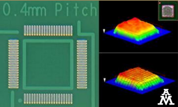
90% on area ratios of 0.50 and a stencil life >8 hours. H10’s powerful wetting characteristics eliminate NWO (HiP) defects and improve pad coverage on all surface finishes. H10 reduces voiding on BGA, BTC and LGA and offers enhanced electrochemical r
New Equipment | Solder Materials
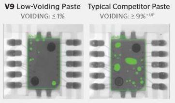
V9 No Clean solder paste is formulated for near-zero voiding on BGA, BTC and LED soldering applications. Significant void reduction achievable on all surface finishes including ENIG, ImSn and OSP. V9 exhibits stable print performance on fine feature
Electronics Forum | Fri Jul 27 09:47:20 EDT 2018 | davef
Adding to Rob's suggestions ... One of the theories about voiding in thermal / ground pads of BTC is: Solder starts melting at the edge of the pad and moves inward towards the center of the solder mass. This traps flux volatilizes. So, there needs t
Electronics Forum | Tue Mar 01 15:13:22 EST 2011 | felixgutierrez
Hi Everyone. I would like your input in regards to lead free solder paste lead free. Which one is the most reliable solder for BGA's and BTC's (QFN). I have used different type of solder and on some of them i get big voids on BTC's and other one i g
Industry News | 2018-08-16 19:58:50.0
The SMTA Capital Chapter is holding its upcoming Capital Expo and Tech Forum at Johns Hopkins University / Applied Physics Lab, Kossiakoff Center, 11100 Johns Hopkins Road, Laurel, MD 20723, on Thursday, August 23rd.
Industry News | 2018-04-11 20:04:01.0
SMTA Europe announces Session 3 Technical Program on Advanced Test Methods at the “Electronics in Harsh Environments Conference” to be held in Amsterdam, Netherlands, on April 25th, 2018.
Technical Library | 2023-01-17 17:25:14.0
BTC Void Reduction For Yield and Performance Enhancement
Technical Library | 2015-07-14 13:19:10.0
Bottom terminated components (BTC) are leadless components where terminations are protectively plated on the underside of the package. They are all slightly different and have different names, such as QFN (quad flat no lead), DFN (dual flat no lead), LGA (land grid array) and MLF (micro lead-frame. BTC assembly has increased rapidly in recent years. This type of package is attractive due to its low cost and good performance like improved signal speeds and enhanced thermal performance. However, bottom terminated components do not have any leads to absorb the stress and strain on the solder joints. It relies on the correct amount of solder deposited during the assembly process for having a good solder joint quality and reliable reliability. Voiding is typically seen on the BTC solder joint, especially on the thermal pad of the component. Voiding creates a major concern on BTC component’s solder joint reliability. There is no current industry standard on the voiding criteria for bottom terminated component. The impact of voiding on solder joint reliability and the impact of voiding on the heat transfer characteristics at BTC component are not well understood. This paper will present some data to address these concerns.

QFN stenicl bumping process demonstrated using a polyimide stencil. This process is one in which a stencil is used to the bump the bottom terminations of a leadless device making it simple to place without voiding of the the thermal pac or shorting o
Events Calendar | Thu Oct 03 00:00:00 EDT 2019 - Thu Oct 03 00:00:00 EDT 2019 | ,
IPC Tech Ed Webinar Series: Ball Grid Array (BGA) and Bottom Termination Component (BTC) Design and Assembly Challenges: Reflow Profiling to Achieve Low Defect Rates and Successful Assembly! – Part 2
SMTnet Express, September 27, 2018, Subscribers: 31,354, Companies: 11,055, Users: 25,237 Assessing the Effectiveness of I/O Stencil Aperture Modifications on BTC Void Reduction Carlos Tafoya, Gustavo Ramirez, Timothy O'Neill; AIM Solder Bottom
. Bottom terminated components (BTC) are le
Surface Mount Technology Association (SMTA) | https://www.smta.org/icehet/workshops.cfm
). - Voids, bridging, and head-in-pillow failures in bottom terminated components (BTC). We will also discuss how artificial intelligence (AI) is changing the way we think about x-ray inspection. Things we would never dream of doing just a few years ago are
PCB Libraries, Inc. | https://www.pcblibraries.com/Forum/when-should-a-pad-use-windowpane-paste-mask_topic2600_post10599.html
air due to the solder migration to one side or the other. You can also solder mask define the thermal pad to prevent solder in vias and reduce or eliminate solder voids due to window-pane. Read this: https


