New Equipment | Solder Materials
Indium Corporation manufactures high quality solder powders and pastes. Powders are available in hundreds of alloys and a full range of sizes. Solder pastes can be made from these powders using a wide variety of flux vehicles to get the best fit for
New Equipment | Rework & Repair Equipment
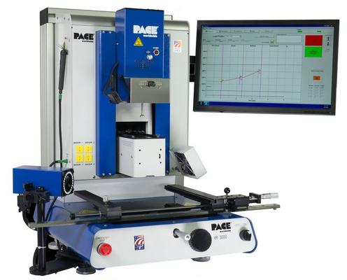
Production BGA Installation & Rework WITHOUT the Expensive Nozzles! The IR 3000 is the most advanced BGA rework system available on the market today. It can easily install and remove BGA, QFN, µBGA/CSP, Flip Chip and other SMD's. Featuring a 500W in
Electronics Forum | Fri May 15 10:04:59 EDT 2009 | aj
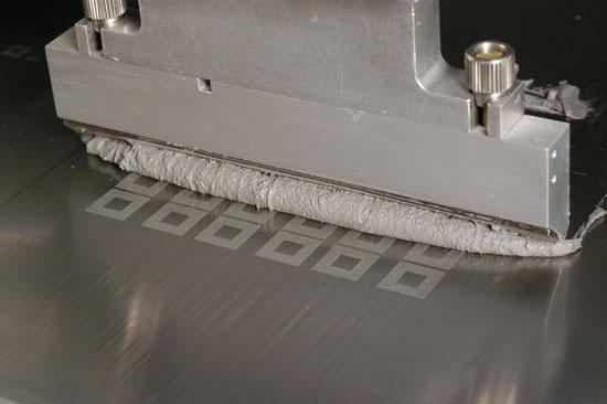
Hi all, Is there any standard for percentage voiding on the center thermal pad on a QFN? We use the dot matrix array for paste to allow for outgassing etc, but we have had a couple of xray inspection "fails" for voiding on this pad , in or around 3
Electronics Forum | Mon Jun 01 16:48:16 EDT 2009 | stevezeva
Mika, Have you ever worked with a 3-row I/O QFN? QFN180 to be exact? Steve
Industry News | 2011-09-14 12:04:43.0
The SMTA announced a session on QFN Assembly and Reliability will take place on Tuesday, October 18 during their annual conference, SMTA International, in Ft. Worth, Texas. Andrew Mawer of Freescale Semiconductor will chair the session and Viswam Puligandla, Ph.D., Nokia (Retired) will co-chair.
Industry News | 2018-08-16 19:58:50.0
The SMTA Capital Chapter is holding its upcoming Capital Expo and Tech Forum at Johns Hopkins University / Applied Physics Lab, Kossiakoff Center, 11100 Johns Hopkins Road, Laurel, MD 20723, on Thursday, August 23rd.
Technical Library | 2019-10-10 00:26:28.0
Voids are a plague to our electronics and must be eliminated! Over the last few years we have studied voiding in solder joints and published three technical papers on methods to "Fill the Void." This paper is part four of this series. The focus of this work is to mitigate voids for via in pad circuit board designs. Via holes in Quad Flat No-Lead (QFN) thermal pads create voiding issues. Gasses can come out of via holes and rise into the solder joint creating voids. Solder can also flow down into the via holes creating gaps in the solder joint. One method of preventing this is via plugging. Via holes can be plugged, capped, or left open. These via plugging options were compared and contrasted to each other with respect to voiding. Another method of minimizing voiding is through solder paste stencil design. Solder paste can be printed around the via holes with gas escape routes. This prevents gasses from via holes from being trapped in the solder joint. Several stencil designs were tested and voiding performance compared and contrasted. In many cases voiding will be reduced only if a combination of mitigation strategies are used. Recommendations for combinations of via hole plugging and stencil design are given. The aim of this paper is to help the reader to "Fill the Void."
Technical Library | 2012-10-18 21:58:51.0
First published in the 2012 IPC APEX EXPO technical conference proceedings. In this paper, we report on a comprehensive study regarding the morphology evolution and voiding of SnAgCu solder joints on the central pad of two different packages – QFN and an Agilent package called TOPS – on PCBs with a Ni/Au surface finish.
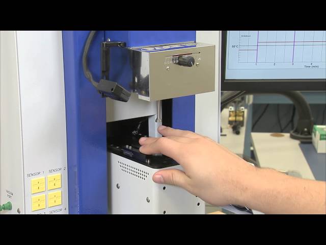
"The IR 3000 offers advanced surface mount rework capability in an integrated, cost-effective, bench-top work station." This video covers the basic processes of the IR 3000, focusing primarily on: Installations, Removals, Component Alignment and Ins
Training Courses | | | PCB Rework and Hand Soldering Courses
The PCB rework and hand soldering courses courses cover techniques of rework and repair of PCBs, BGAs and other electronics assemblies, and teach fundamentals of soldering of electronics assemblies.
Training Courses | | | PCB Rework and Hand Soldering Courses
The PCB rework and hand soldering courses courses cover techniques of rework and repair of PCBs, BGAs and other electronics assemblies, and teach fundamentals of soldering of electronics assemblies.
Voiding Control for QFN Assembly Voiding Control for QFN Assembly Quad Flat No Leads (QFN) package designs receive more and more attention in electronic industry nowadays. This package offers a number of benefits including (1) small size
SMTnet Express, October 3, 2018, Subscribers: 31,373, Companies: 11,056, Users: 25,258 Fill the Void II: An Investigation into Methods of Reducing Voiding Tony Lentz - FCT Assembly , Patty Chonis, JB Byers - A-Tek Systems Voids in solder joints
Heller Industries Inc. | https://hellerindustries.com/intermetallics-growth/
& Technical Articles Videos THERMAL PROCESS SOLUTIONS Reflow Soldering Solutions Causes & Defects – Reflow Soldering Solder Ball Defects Insufficient Solder Wicking Defects Tombstoning PCB Soldering PCB Bridging Defects PCB Dewetting PCB Nonwetting Circuit Board Voids Intermetallic Growth on PCB
Surface Mount Technology Association (SMTA) | https://www.smta.org/knowledge/webinars.cfm
Jennie Hwang, Ph.D. $200.00 2015 Shining a Light on LED Technology Martine Simard-Normandin Free! 2015 Process Optimization and Defect Elimination for PCB Assembly Tim Jensen $200.00 2015 Thermal Events

COT specializes in high quality SMT nozzles and consumables for pick and place machines. We provide special engineering design service of custom nozzles for those unique and odd components.
2481 Hilton Drive
Gainesville, GA USA
Phone: (770) 538-0411


