Industry Directory | Manufacturer
a leading manufacturer of wafer handling tools for the global semiconductor industry. Our products include vacuum wands, wafer tweezers, HEPA vacuum pumps, etc. ESD safe products and tools for 300mm wafers are also available.
Industry Directory | Manufacturer
CVInc services advanced packaging. Placing solder bumps on single die, partial wafers, and complete wafers...we also offer RDL (redistribution) services in 5-7 working days. Our custom preforms are as small as 50um geometries.
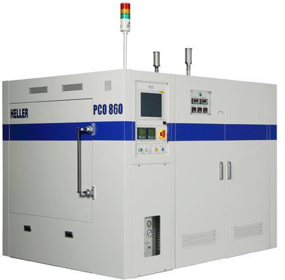
New Equipment | Curing Equipment
A Pressure Cure Oven (PCO), or Autoclave, is used to minimize voiding and increase adhesion strength for bonding processes typically used in die attach and underfill applications. PCO pressurizes air into a rigid vessel and heats & cools with
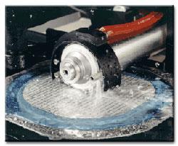
Our fully automated silicon wafer dicing service consistently meet the tight requirements expected in our industry and demanded by our customers. At Syagrus Systems, we know that a good wafer dicing or wafer cutting process sets the pace for all rema
Electronics Forum | Wed Sep 13 07:17:32 EDT 2000 | Paul Gerits
Dear Sir, It is possible depending on the exact application. At the moment only way to go direct from die to waffle or PCB is with Hover Davies direct die feeders on Philips EMT (ACM, advanced component mounter), Universal and Siemens machines. This
Electronics Forum | Tue Sep 12 03:36:50 EDT 2000 | PeterB
I have just read that Hover-Davis now manufacture a direct die feeder which can feed directly from wafer to P & P machine compatible with a number of different placement machine manufacturers. Perhaps this will help? Best regards
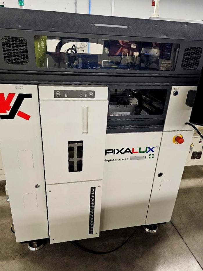
Used SMT Equipment | Pick and Place/Feeders
K&S PIXALUX High Speed LED Placement Machine Model: PIXALUX Year: 2018 Micro & Mini LED Placement High productivity and yield with its ultrafast placement head design Placement accuracy and speed on multiple types of substrates Supports placement o
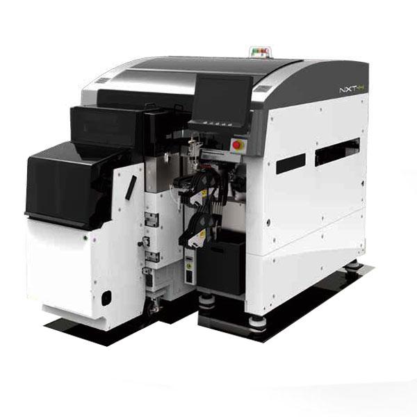
Used SMT Equipment | Chipshooters / Chip Mounters
NXT-H and NXT-Hw support placing small LEDs and bare dies at high-speed as well as performing hybrid production including flip chips.Fuji Ultra Accurate Placement Platform.Hybrid placement of wafers and SMDs. Wafer and reel part placement in a single
Industry News | 2003-04-29 07:30:06.0
Announce their plans to co-sponsor a free online conference on the current state of bare die packaging
Industry News | 2018-02-02 18:44:38.0
The IWLPC Technical Committee is pleased to announce the Best of Conference, Best Presentation & Best Papers in WLP, 3D, Advanced Manufacturing and Test tracks as chosen by the technical committee and attendees based on technical merit, relevance, originality, knowledge of subject, quality of material, and quality of presentation.
Technical Library | 1999-05-07 10:14:57.0
This paper describes a model developed to calculate number of redundant good die per wafer. A block redundancy scheme is used here, where the entire defective memory subarray is replaced by a redundant element. A formula is derived to calculate the amount of improvement expected after redundancy. This improvement is given in terms of the ratio of the overall good die per wafer to the original good die per wafer after considering some key factors.
Technical Library | 2020-05-26 22:28:56.0
Both the number and the variants of Ball Grid Array packages (BGAs) are tending to increase on network Printed Board Assemblies (PBAs)with sizes ranging from a few mm die size Wafer Level Packages (WLPs) with low ball count up to large multi-die System-in-Package (SiP) BGAs with 60-70 mm side lengths and thousands of I/Os.

General curing, die attach curing, underfill curing, film & tape bonding, wafer laminating.

ACI Technologies Inc. (ACI) is a scientific research corporation dedicated to the advancement of electronics manufacturing processes and materials for The Department of Defense and industry. This video provides an overview of our commercial service
Training Courses | | | PCB Design Courses
The PCB design courses teach students the process, techniques and tools needed to design layout of printed circuit boards.
Events Calendar | Mon Apr 23 00:00:00 EDT 2018 - Thu Apr 26 00:00:00 EDT 2018 | Shanghai, China
SMTA China East Conference 2018
Events Calendar | Wed Oct 23 00:00:00 EDT 2019 - Thu Oct 24 00:00:00 EDT 2019 | Guadalajara, Mexico
SMTA Mexico Expo 2019
Career Center | South Plainfield, New Jersey USA | Sales/Marketing,Technical Support
Alpha, a business unit of Alent plc and the global leader in the development, manufacturing and sales of innovative specialty materials used in a wide range of industry segments, including electronics assembly, power electronics, die attach, LED ligh
Career Center | , South Carolina | Engineering
Assembly engineer with leadership capabilities needed for this position. Implement the proper controls to assure a reliable operation of the strap/inlay assembly, strap attach, and slitting processes. Actively pursue opportunities to continually imp
Career Center | Melbourne, Florida USA | Management,Production,Quality Control
Technical Skills/Abilities: � Management � Quality Assurance � Strong Troubleshooting Skills � Strategic Planning � Employee Training � Quality Assurance � Problem Resolution � Mechanical/Technical Aptitude
Career Center | Cavite, Philippines | Engineering,Technical Support
I had 15 years Handling SMT Equipment.
Wafer-Level Packaged MEMS Switch With TSV Wafer-Level Packaged MEMS Switch With TSV by: Nicolas Lietaer, Thor Bakke, Anand Summanwar; SINTEF , Per Dalsjø, Jakob Gakkestad; Norwegian Defence Research Establishment (FFI), Frank Niklaus; KTH - Royal
ASYMTEK Products | Nordson Electronics Solutions | https://www.nordson.com/de-DE/divisions/dage/wafer-inspection-and-metrology
für die Inspektion auf Wafer-Ebene mit branchenführender Vergrößerung und Bildqualität. Laden Sie Wafer manuell und prüfen Sie mit der intuitiven, schnell zu erlernenden Gensys™
GPD Global | https://www.gpd-global.com/co_website/pcdpumpseries-underfill-small.php
Underfill Fluid Dispense on 6 mm Die Home Products Fluid Dispense Systems High Precision Dispenser - MAX Series Large Format Board Processing - DS Series Table Top Manufacturing Loader


