Industry Directory | Distributor / Manufacturer
Lorlin manufactures discrete semiconductor component test systems for small signal and power devices. 50 years in business, over 3000 installations. SMD devices: transistors, Fets, diodes, scrs, triacs, optos, and many others.
WENADE TECHNOLOGY remarkets GOOD USED equipment to the electronics industry, initially concentrating on the Semiconductor sector and gradually encompassing the Test (and ATE related); Wafer Fab; and PCB Assembly sectors of the same industry.

New Equipment | Fabrication Services
Aluminum PCB & Metal Core PCB & LED PCB Circuit board Aluminium PCB are metal-based, copper-clad laminates with a good heat dissipation function. Usually, Aluminium PCB is refer to LED PCB board, which is the most important part of LED display and l
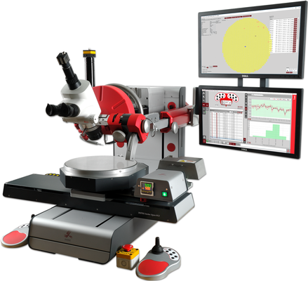
New Equipment | Test Equipment - Bond Testers
Fully integrated solution for automated wafer testing (up to 300 mm). The Condor Sigma W12 is specifically designed for precision shear testing and Cold Bump Pull (CBP) on wafer or at wafer level. The system has the largest X/Y and fastest stages av
Electronics Forum | Fri Nov 10 12:22:12 EST 2000 | casi
I'm interested in probes for wafer testing made in verted. I need to tested wafers with pad with flat gold bumps ( 17um ) with pitch = 70um. I'm also interested in every web site related on gold bumps testing. Thanks a lot !!! Casi
Electronics Forum | Mon Jun 05 05:41:48 EDT 2000 | casi
I need to find info about testing and probe contact about wifers with bump on pads. Thanks a lot to everybody that helps me
Used SMT Equipment | SMT Equipment
Auction: Phoenix X-Ray PCB Analyser, Wafer Probers, Test Chambers, Hot Bar Bonders, Dicing Saws & More Featuring: BAE - Manassas, Virginia USA • V.J. Technologies VJ-1000 X-Ray System A World Class Semiconductor Mfg. Co. - Hayward, California USA
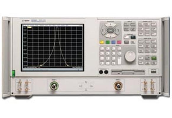
Used SMT Equipment | General Purpose Test & Measurement
The ENA Series covers the frequency range of 300 kHz to 8.5 GHz, and is available in 2, 3 and 4 port models. The PNA-L Series offers the key features of the RF PNA and is code-compatible with the RF PNA. The PNA-L Series covers the frequency range of
Industry News | 2002-03-29 08:28:28.0
Has Found a Buyer for its Wafer Fabrication Facility in Plymouth, England
Industry News | 2019-07-16 19:36:51.0
The Surface Mount Technology Association (SMTA) and Chip Scale Review are pleased to announce the program for the 16th annual International Wafer-Level Packaging Conference (IWLPC). The conference will be held October 22-24, 2019 at the DoubleTree by Hilton Hotel in San Jose, California.
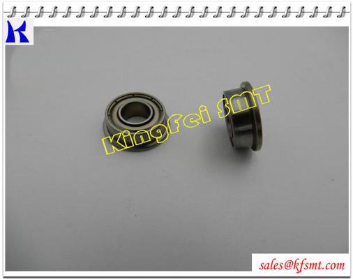
Parts & Supplies | Assembly Accessories
SMT MACHINE GENUINE JUKI SPARE PARTS JUKI 2050 2060 FX-1 BEARING SB106001900 JUKI Pats Specifications: Brand Name JUKI 2050 2060 FX-1 BEARING Part number SB106001900 Model JUKI SMT MACHINE SPARE PARTS Ensure Test in machine confirmation G
Parts & Supplies | SMT Equipment
Specifications: Brand Name JUKI PLASTIC RAIL Part number 40046786 Model TSUBAKI TKP0450 58B R95 Ensure Test in machine confirmation Guarantee 1 month usage for machine FX-3 FX-3R Supply all JUKI motors at lower price JUKI 40034750 R3
Technical Library | 2010-06-23 21:59:03.0
Quality control is one of the main bottlenecks in the production of micro-opto-electromechanical systems/microelectromechanical systems (MOEMS/MEMS) because each structure on a wafer is serially inspected and scanned stepwise over the entire wafer area.
Technical Library | 1999-08-05 10:45:36.0
In 1998, the International 300 mm Initiative (I300I) demonstration and characterization programs will focus on 180 nm technology capability. To support these activities, I300I and equipment supplier demonstration partners must use starting silicon wafers with key parameters specified at a level appropriate level for 180 nm processing, including contamination and lithographic patterning. This document describes I300I's silicon wafer specifications, as developed with the I300I Silicon Working Group (member company technical advisors) and SEMI Standards.
Why you should attend International Wafer-Level Packaging Conference, October 23 - 25, 2018 in San Jose, California, USA.

ACI Technologies Inc. (ACI) is a scientific research corporation dedicated to the advancement of electronics manufacturing processes and materials for The Department of Defense and industry. This video provides an overview of our commercial service
Training Courses | | | PCB Design Courses
The PCB design courses teach students the process, techniques and tools needed to design layout of printed circuit boards.
Events Calendar | Tue Feb 15 00:00:00 EST 2022 - Thu Feb 17 00:00:00 EST 2022 | San Jose, California USA
Wafer-Level Packaging Symposium
Events Calendar | Wed Feb 14 00:00:00 EST 2024 - Fri Feb 16 00:00:00 EST 2024 | San Francisco, California USA
Wafer-Level Packaging Symposium
Career Center | South Plainfield, New Jersey USA | Sales/Marketing,Technical Support
Alpha, a business unit of Alent plc and the global leader in the development, manufacturing and sales of innovative specialty materials used in a wide range of industry segments, including electronics assembly, power electronics, die attach, LED ligh
Career Center | San Jose, California USA | Engineering
www.srqconsultants.com : for all Job Reqs This Analog IC Test Development Engineer position will require senior level ability on at least one of the following machines: Teradyne: Catalyst, A5XX, J750, Tiger Agilent 84000, 94000 Credence Duo, Quarte
Career Center | Botevgrad, Sofia Bulgaria | Engineering,Production,Quality Control,Research and Development,Sales/Marketing
AOI - Omron RNS/RNS_ptH, VI3000, Marantz 22X IPC-610D Class 3, Pb/Pb free process, 5S, FMEA, MSA, PPAP, SPC, CPK, 6Sigma, lean manufacturing, Quality management, ISO/TS 16949 ,ISO 9001,ISO 14 001
Career Center | Botevgrad, Sofia Bulgaria | Engineering,Production,Quality Control
AOI - Omron RNS_ptH, RNS-LS, VT-WIN2 VI3000 Marantz 22X IPC 610D certified ISO 9001-2008, etc automotive standards ROHS
Reliability Enhancement of Wafer Level Packages with Nano-Column-Like Hollow Solder Ball Structures Reliability Enhancement of Wafer Level Packages with Nano-Column-Like Hollow Solder Ball Structures by: Ronak Varia, Xuejun Fan; Lamar University
Wafer-Level Packaged MEMS Switch With TSV Wafer-Level Packaged MEMS Switch With TSV by: Nicolas Lietaer, Thor Bakke, Anand Summanwar; SINTEF , Per Dalsjø, Jakob Gakkestad; Norwegian Defence Research Establishment (FFI), Frank Niklaus; KTH - Royal
ASYMTEK Products | Nordson Electronics Solutions | https://www.nordson.com/en/products/bondtesters?con=t&page=8
Bondtesters – Bonding Test Equipment - Wafer Tests | Nordson Nordson Corporation Global Directory | Languages NASDAQ $230.50 -0.49 Our Products Our Industries Our Applications Brands
Surface Mount Technology Association (SMTA) | https://www.smta.org/knowledge/proceedings_abstract.cfm?PROC_ID=4798
BTC/QFN Test Board Design Considerations and Method for Qualifying Soldering Materials and Cleaning Processes 中文 MEMBERS LOGIN Membership Become a Member


