Next Scheduled Public Courses: May 6, 2008 ~ Dallas, TX May 7, 2008 ~ Singapore May 8, 2008 ~ Penang, Malaysia May 14, 2008 ~ Las Vegas May 14, 2008 ~ Boston, MA June 11, 2008 ~ Hsin-Chu, Taiwain July 18, 2008 ~ San Francisco, CA August 8, 2008 ~ S
New Equipment | Test Equipment
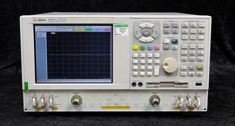
The Agilent E8358A vector network analyzer is a member of the PNA Series network analyzer platform and provides the combination of speed and precision required for testing components. The PNA Series meets this testing challenge by providing the right
Electronics Forum | Mon Sep 11 00:31:13 EDT 2000 | rcsantos
Is there somebody who knows if there is a machine already available in market that can transfer die from wafer to waffle tray. This machine should a stand alone type or can be integrated to some P&P machine. What I'm trying to say is just like the on
Electronics Forum | Tue Sep 12 03:36:50 EDT 2000 | PeterB
I have just read that Hover-Davis now manufacture a direct die feeder which can feed directly from wafer to P & P machine compatible with a number of different placement machine manufacturers. Perhaps this will help? Best regards
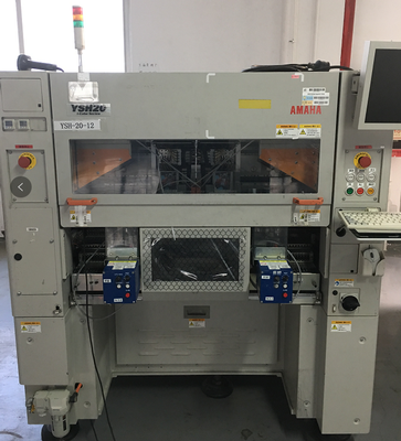
Used SMT Equipment | Chipshooters / Chip Mounters
Dear All , We currently have 3 units YSH20 available in our stock, if you have any interesting, please contact me. Applicable PCB L50 x W30 to L250 x W200mm ****Up to L340 x W340mm" is applicable. Please contact us separately. Mounting c
Industry News | 2002-03-29 08:28:28.0
Has Found a Buyer for its Wafer Fabrication Facility in Plymouth, England
Industry News | 2007-10-04 17:21:57.0
SARASOTA, FL � September 27, 2007 � Inovaxe Corp., a leader in delivering supply chain management solutions to electronics manufacturers, announces that it will exhibit both a one- and a two-bay INOCART material handling system (INOCART-2BAY) in booth 618 at the upcoming SMTA International exhibition and conference, scheduled to take place October 7-11, 2007, in Orlando, FL.
Technical Library | 2016-08-11 15:49:59.0
The challenge for 3D IC assembly is how to manage warpage and thin wafer handling in order to achieve a high assembly yield and to ensure that the final structure can pass the specified reliability requirements. Our test vehicles have micro-bumped die having pitches ranging from 60um down to 30um. The high density of pads and the large die size, make it extremely challenging to ensure that all of the micro-bump interconnects are attached to a thin Si-interposer. In addition, the low standoff between the die and interposer make it difficult to underfill. A likely approach is to first attach the die to the interposer and then the die/interposer sub-assembly to the substrate. In this scenario, the die/interposer sub-assembly is comparable to a monolithic silicon die that can be flip chip attached to the substrate. In this paper, we will discuss various assembly options and the challenges posed by each. In this investigation, we will propose the best method to do 2.5D assembly in an OSAT(Outsourced Assembly and Test) facility.
Technical Library | 2020-09-02 22:02:13.0
With the adoption of Wafer Level Packages (WLP) in the latest generation mobile handsets, the Printed Circuit Board (PCB) industry has also seen the initial steps of High Density Interconnect (HDI) products migrating away from the current subtractive processes towards a more technically adept technique, based on an advanced modified Semi Additive Process (amSAP). This pattern plate process enables line and space features in the region of 20um to be produced, in combination with fully filled, laser formed microvias. However, in order to achieve these process demands, a step change in the performance of the chemical processes used for metallization of the microvia is essential. In the electroless Copper process, the critical activator step often risks cross contamination by the preceding chemistries. Such events can lead to uncontrolled buildup of Palladium rich residues on the panel surface, which can subsequently inhibit etching and lead to short circuits between the final traces. In addition, with more demands being placed on the microvia, the need for a high uniformity Copper layer has become paramount, unfortunately, as microvia shape is often far from ideal, the deposition or "throw" characteristics of the Copper bath itself are also of critical importance. This "high throwing power" is influential elsewhere in the amSAP technique, as it leads to a thinner surface Copper layer, which aids the etching process and enables the ultra-fine features being demanded by today's high end PCB applications. This paper discusses the performance of an electroless Copper plating process that has been developed to satisfy the needs of challenging amSAP applications. Through the use of a radical predip chemistry, the formation, build up and deposition of uncontrolled Pd residues arising from activator contamination has been virtually eradicated. With the adoption of a high throwing power Copper bath, sub 30um features are enabled and microvia coverage is shown to be greatly improved, even in complex via shapes which would otherwise suffer from uneven coverage and risk premature failure in service. Through a mixture of development and production data, this paper aims to highlight the benefits and robust performance of the new electroless Copper process for amSAP applications

The Microelectronics Lab was established to meet the rising need for advanced systems development and packaging to address the emerging challenges and issues facing today’s electronics assemblies. Advanced design and modeling software enables STI to

This is the first in a series of 10-minute videos to introduce new users to the basics of machine vision technology. In this video, users will learn what machine vision is, how it is used in factory automation, and its four most common applications.
GPD Global | https://www.gpd-global.com/pdf/pbt/Wafer-Option-PBFT-PBT-3000M.pdf
-global.com Figure A-B Top view of Wafer Option and valve size indicators; from left to right, the valves are designated as 30 mm, 20 mm, and 10 mm
ASYMTEK Products | Nordson Electronics Solutions | https://www.nordson.com/en/divisions/dage/wafer-inspection-and-metrology
. All th e benefits and performanc e of Quadra 7, with integrated wafer handling. Quadra W8 allows operators to inspect wafers directly from the FOUP without needing to handle the wafer

.gif)


