New Equipment | Test Equipment
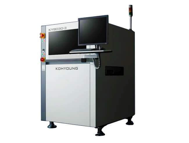
Koh Young KY8030-3 3D Inline SPI component Range: 01005 PCB size:350x330mm Dimension:1000x1335x1627mm weight:800kg Product description: Koh Young KY8030-3 3D Inline SPI, component Range: 01005, PCB size:350x330mm, Dimension:1000x1335x1627mm, weight:
New Equipment | Test Equipment
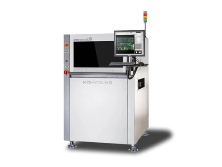
KOH YOUNG Zenith UHS 3D AOI Camera: 12M 15um Max PCB: 490 x 510 mm Weight: 600kg Dimension: 820x1265x1627 mm KOH YOUNG Zenith UHS 3D AOI KOH YOUNG Zenith UHS 3D AOI A model with 8 projections and an 8MPx camera. This model is very resistant t
Electronics Forum | Wed Mar 28 11:29:49 EST 2001 | gcs
I've used below: WEIGTH OF COMPONENT IN GRAMS ---------------------------- TOTAL PAD MATING AREA IN SQUARE INCHES GRAMS PER SQUARE INCH MUST BE EQUAL/GREATER THAN 30 FOR SECONDARY MOUNTING.
Electronics Forum | Thu Oct 15 11:04:28 EDT 2009 | spitkis2
Thanks Jim. Pressing the QFN into paste was what I thought of, just wasn't sure if it would cause solder paste to be pressed outside the pad area and possibly bridge with an adjacent pad. Do you recall the ratio of paste coverage to the pad area?
Used SMT Equipment | Screen Printers
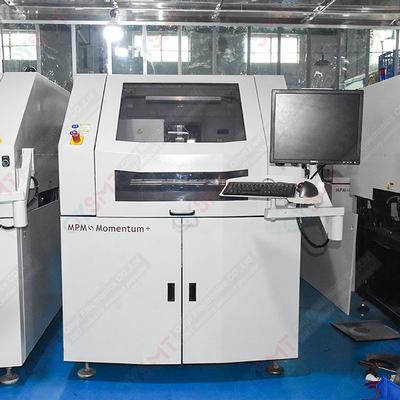
Momentum was designed and built to be a no-nonsense production machine. Cost-efficient and featuring a modest footprint, it grows with the user; innovative patented features can be added on or retrofitted as needed as the user’s throughput dema
Used SMT Equipment | Screen Printers
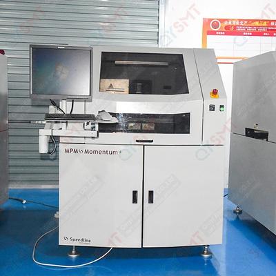
Momentum was designed and built to be a no-nonsense production machine. Cost-efficient and featuring a modest footprint, it grows with the user; innovative patented features can be added on or retrofitted as needed as the user’s throughput dema
Industry News | 2018-12-08 03:29:29.0
SMT Dictionary – Surface Mount Technology Acronym and Abbreviation

Parts & Supplies | SPI / Solder Paste Inspection
Quick programming, friendly programming interface Multiple measurement methods True one-button measurement Eight-way motion button, one-click focus Adjustable scanning pitch Solder paste 3D simulation function Powerful SPC function MARK
_1.jpg)
Parts & Supplies | Pick and Place/Feeders
JUKI FEEDER part E513070600B E9630729000 T AC SERVO MOTOR(TS4632N2020E600) E9630755000 RERAY UNIT E96307800A0 HEAD SENSOR ASM E963171500A DUCT (KD-76-03-C) E963171500B DUCT (KD-76-045-C) E963171500C DUCT (KD-76-085-C) E9631721000 LAHD SENSOR
Technical Library | 2017-09-28 16:36:33.0
These nano-coatings also refine the solder paste brick shape giving improved print definition. These two benefits combine to help the solder paste printing process produce an adequate amount of solder paste in the correct position on the circuit board pads. Today, stencil aperture area ratios from 0.66 down to 0.40 are commonly used and make paste printing a challenge. This paper presents data on small area ratio printing for component designs including 01005 Imperial (0402 metric) and smaller 03015 metric and 0201 metric chip components and 0.3 mm and 0.4 mm pitch micro BGAs.

Inline 3D SPI, Standard Automatic solder paste inspection system As one of the strongest SMT 3D SPI Manufacuturer in China, we provide you all the different models of online solder paste inspection machine,we have variety of size and models of the
Substrate processing: Maximum substrate size (XxY): 609.6mmx508mm(24”x20”) For circuit boards larger than 20”, special fixtures are required Minimum substrate size (XxY): 50.8mmx50.8mm(2”x2”)
Career Center | Bangalore, India | Engineering,Maintenance,Production,Technical Support
SMT Stencil designing & Knowledge of full SMT process software known CAD/CAM -circuit CAM Pro 7.3,GC Power station, GCCAM Edit,Auto CAD, Fault finding of Electronic Boards & Servicing electronic machines.
SMTnet Express, September 28, 2017, Subscribers: 30,862, Companies: 10,741, Users: 23,873 An Investigation into the Use of Nano-Coated Stencils to Improve Solder Paste Printing with Small Stencil Aperture Area Ratios Jasbir Bath, Tony Lentz, Greg
PCB Libraries, Inc. | https://www.pcblibraries.com/forum/ipc2221-2222-and-throughhole-pad-stacks_topic2586_post10872.html
a copper plane and not intrude into the anti-pad area. Therefore, make the anti-pad large enough to manufacture but small enough to maintain signal integrity. Note: The OD of the plane Thermal Relief is the same diameter as the plane Anti-pad
| https://www.eptac.com/soldertips/soldertips-issues-with-incomplete-solder-reflow-in-production-2/
: I’m not exactly sure of what you mean by flux exhaustion, however; my interpretation is, there wasn’t enough flux in the solder paste to prepare the pad/land area and have the molten solder flow over the complete pad or land area itself


winsouce.jpg)