Industry Directory | Manufacturer
The exclusive supplier of SIPAD Solid Solder Deposit in North America and the only SIPAD Solid Solder Deposit (SSD) coating service bureau in the world.
New Equipment | Solder Paste Stencils
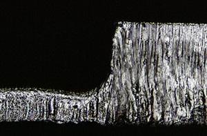
Through the increase of mixed technologies, stepped stencils have gained importance to the electronic assembly manufacturer. If the solder paste quantity can no longer be adequately regulated by adjusting Step/Relief Stencil Picture the pad sizes, st

New Equipment | Rework & Repair Services
Specifications: 1.WDS-700 bga rework station 2.Optical alignment 3.Automatic machine 4.MCGS touch screen 5.CE,ISO passed 6.Small size Sole manufacturer WDS-700 automatic optical alignment mobile phone BGA rework station with HD camera Our
Electronics Forum | Wed Nov 07 11:56:44 EST 2001 | mparker
Pad spacing is just one element to consider. Your pad spacing is determined by the pitch (center to center distance between the leads). There are several good resources to find the appropriate pitch per device. Search the archives here or refer to th
Electronics Forum | Mon Aug 16 04:47:04 EDT 1999 | Charles Stringer
| | | One of the DFM suggestions I've seen is to remove the solder mask web, i.e. the mask between pads on 20-mil QFP devices. The rational is that if the mask is thicker than the pad the mask can prevent the stencil from making intimate contact wit
Industry News | 2003-03-21 08:12:24.0
Tecan reckons it is consistently producing what may be regarded as the most efficient stencils in the world today.
Industry News | 2018-12-08 03:29:29.0
SMT Dictionary – Surface Mount Technology Acronym and Abbreviation

Parts & Supplies | SPI / Solder Paste Inspection
Quick programming, friendly programming interface Multiple measurement methods True one-button measurement Eight-way motion button, one-click focus Adjustable scanning pitch Solder paste 3D simulation function Powerful SPC function MARK
Technical Library | 2009-05-14 13:57:43.0
Is screen printing technology able to keep pace with rising quality demands and increasingly complex board layouts? Or, is new jet printing technology ready to fill the gap? A comparison study between the two methods reveals some interesting differences. Screen printers offer some possibilities for optimizing solder paste deposits, but optimization is far easier and quicker with the jet printer. At the same time, the ability to print individualized deposits on every single pcb pad may be the ultimate answer to the growing quality challenge.

I.C.T Provide SMT Production Line solutions with Automated Optical Inspection (AOI) AOI is short for Automated Optical Inspection, which is widely used in the electronics industry to check the appearance of PCBA assembly at the back end of the cir
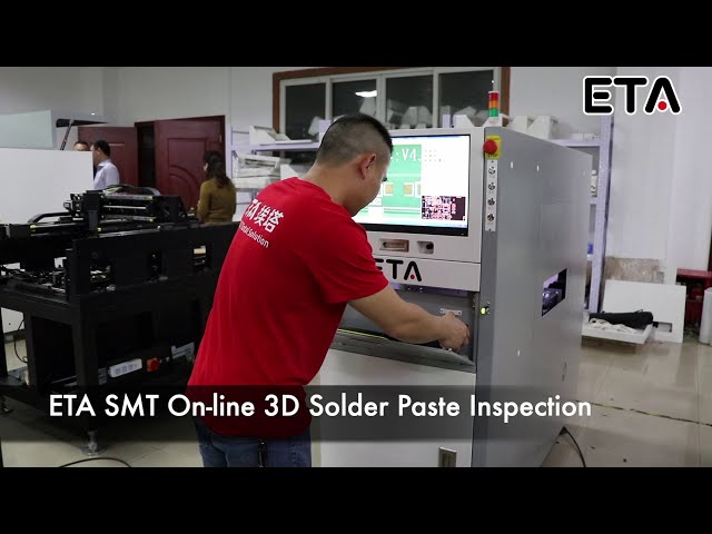
SMT On-line 3D Solder Paste Inspection If you could not find any similar items you want, you may send some photos to us. because our catalog and website haven't included all of our products. solder paste inspection,SMT SPI,SPI machine, SPI in
| https://www.feedersupplier.com/sale-13018909-smt-koh-young-ky8030-3-spi-inspection-machine.html
.) Min.Distance between Paste Deposit 100um(3.94mils) 150um(5.91mils) 200um(7.87mils) Camera 4M Pixel Camera IIIumination lR-RGB LED Dome Styledlllumination Z Resolution
PCB Libraries, Inc. | https://www.pcblibraries.com/forum/topic780&OB=ASC.html
. keyboard shortcut = d Advantage: User can quickly measure distances between pads, keep outs, solder masks, and other features to check and review if the footprint is correct. in distance mode


