Industry Directory | Research Institute / Laboratory / School / Manufacturer
Manufacturer of surface deposition and plasma surface cleaning and etching equipment offering reliable, repeatable cleaning and etching of PCBs and other materials.
Industry Directory | Manufacturer
Enercon manufactures induction cap sealers which are recognized around the world for providing tamper evidence, preventing leaks and preserving freshness with hermetic seals for packagers of food, beverage, pharmaceuticals, ...
New Equipment | Rework & Repair Equipment
BEST HotDots™ are designed to simply and cleanly attach jumper wires on a board. HotDots™ are built to survive at high temperature as both the adhesive and the polyimide material are designed to withstand wash and reflow temperatures. HotDots™ are a

New Equipment | Soldering Robots
Description: Spot-welding and drag soldering is available Function: Soldering all kinds of plug-in electronic components, such as capacitor,resistor,pin header,pin wire, LCD through hole Feature: 1. Has spot-welding,drag soldering, automati
Used SMT Equipment | Semiconductor & Solar
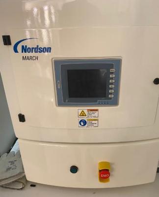
Nordson MARCH AP-300 Plasma System Cleaner 100-230VAC, 50/60Hz, 3.5A @208V, Single Phase A compact and benchtop model, the Nordson March plasma system AP-300 has a volume capacity of 33.1 liters, supported by up to seven (7) adjustable shelves in
.JPG)
Used SMT Equipment | Adhesive Dispensers
Asymtek Millennium 600 Epoxy Dispenser For Sale Vintage 1998 Integrated mass flow calibration system automatically compensates for changes in fluid viscosity Full temperature control of fluid delivery with closed-loop substrate heating to
Industry News | 2024-03-11 15:00:03.0
Connect with our experts and see plasma and dispensing equipment for microelectronics manufacturing in booth 3645
Industry News | 2014-10-16 19:22:45.0
Industry-leading associations IPC and SMTA jointly announce the High-Reliability Cleaning and Conformal Coating Conference scheduled to take place November 18-20, 2014 at the Chicago Marriott in Schaumburg, IL.
Technical Library | 2020-08-27 01:22:45.0
Initially adopted internal specifications for acceptance of printed circuit boards (PCBs) used for wire bonding was that there were no nodules or scratches allowed on the wirebond pads when inspected under 20X magnification. The nodules and scratches were not defined by measurable dimensions and were considered to be unacceptable if there was any sign of a visual blemish on wire-bondable features. Analysis of the yield at a PCB manufacturer monitored monthly for over two years indicated that the target yield could not be achieved, and the main reasons for yield loss were due to nodules and scratches on the wirebonding pads. The PCB manufacturer attempted to eliminate nodules and scratches. First, a light-scrubbing step was added after electroless copper plating to remove any co-deposited fine particles that acted as a seed for nodules at the time of copper plating. Then, the electrolytic copper plating tank was emptied, fully cleaned, and filtered to eliminate the possibility of co-deposited particles in the electroplating process. Both actions greatly reduced the density of the nodules but did not fully eliminate them. Even though there was only one nodule on any wire-bonding pad, the board was still considered a reject. To reduce scratches on wirebonding pads, the PCB manufacturer utilized foam trays after routing the boards so that they did not make direct contact with other boards. This action significantly reduced the scratches on wire-bonding pads, even though some isolated scratches still appeared from time to time, which caused the boards to be rejected. Even with these significant improvements, the target yield remained unachievable. Another approach was then taken to consider if wire bonding could be successfully performed over nodules and scratches and if there was a dimensional threshold where wire bonding could be successful. A gold ball bonding process called either stand-off-stitch bonding (SSB) or ball-stitch-on-ball bonding (BSOB) was used to determine the effects of nodules and scratches on wire bonds. The dimension of nodules, including height, and the size of scratches, including width, were measured before wire bonding. Wire bonding was then performed directly on various sizes of nodules and scratches on the bonding pad, and the evaluation of wire bonds was conducted using wire pull tests before and after reliability testing. Based on the results of the wire-bonding evaluation, the internal specification for nodules and scratches for wirebondable PCBs was modified to allow nodules and scratches with a certain height and a width limitation compared to initially adopted internal specifications of no nodules and no scratches. Such an approach resulted in improved yield at the PCB manufacturer.
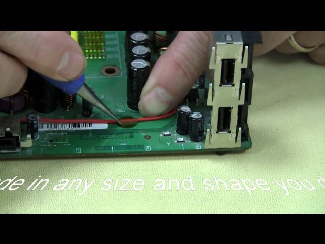
This video demonstrated the use of BEST Inc HotDots(TM) which allow wires to be affixed to the PCB or other surfaces-even when those surfaces go through reflow. There are other similar products out there but none of which can be readily customized no

The BT-1 Plasma Etch System is fully automated and is capable of processing large quantities of parts up to 21"x21" for substrate cleaning and surface modification applications prior to bonding applications. VISIT THE PLASMA ETCH WEBSITE FOR MORE IN
Career Center | Boulder, Colorado USA | Engineering,Production,Quality Control
Senior-level micro-electronic technician capable of independent manufacture of custom hybrids, focal plane assemblies, and prototype detector assemblies in cleanroom environment (in Advanced Packaging and Detector Laboratory). MINIMUM QUALIFICATIONS
Career Center | Brooklyn, New York USA | Engineering,Production
Mini-Circuits designs, manufactures and distributes integrated circuits, modules, and sub-systems for high performance radio frequency (RF) and microwave applications. With design, sales and manufacturing locations in over 30 countries, Mini-Ci
Career Center | Sto. Tomas, Batangas, Philippines | Engineering
SKILLS & EXPERIENCES A.Materials engineering and management 1.Handles matters about materials -Ceramic and laminate substrates & Surface Mount Devices (SMDs) i.e. chip capacitors and resistors -Perishable materials i.e. solder paste (including Pb-fr
Career Center | San Isidro Cabuyao Laguna, Philippines | Engineering,Maintenance,Production,Technical Support
Duties & Responsibilities (Equipment Technician): Production line support, conduct setup and troubleshooting on handled machines such as COB and backend equipment. Conduct Preventive maintenance
SMT Express, Volume 2, Issue No. 9 - from SMTnet.com Volume 2, Issue No. 9 Thursday, September 14, 2000 Featured Article Return to Front Page Book Review Reviewed by Dave Fish (davef ), Pandion Electronics, Inc Title: Wire Bonding
| https://www.eptac.com/faqs/ask-helena-leo/ask/gold-wire-bond-failing-pull-test
: We have a situation where we have gold boards which accept gold wire bonding, but are failing a pull test. Other than making sure the boards are clean with a quick trip into the degreaser, is there any other way to refresh gold... Question
| https://www.smtfactory.com/What-is-an-LED-Flip-Chip-id3680601.html
. SMT PRODUCTION LINE CONTACT US You are here: Home » News & Events » What is an LED Flip Chip? What is an LED Flip Chip? Views: 0 Author: I.C.T Publish Time: 2021-01-15 Origin: www.smtfactory.com Inquire Industry Introduction LED flip chip refers to the chip that can be directly bonded with ceramic substrate without welding wire


.gif)