Industry Directory | Manufacturer
US manufacturer of metallized ceramic substrates & packages; specializing in PCTF (plated copper over thick film) & low cost AgENIG (silver with electroless nickel and immersion gold plating).
High Tech, Quick Turn, Manufacturer of PCB's up to 44 layer count. Specializing in Prototype and R&D. Mil-Spec 31032 & 55110 Certified. Located in Fremont, CA & Amesbury, MA.
New Equipment | Education/Training
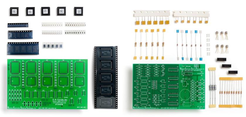
BEST training kits feature REAL circuit boards that represent actual soldering conditions. These training kits feature ".062 thick multilayer boards which are more representative of the thermal conditions of "real" circuit boards. This board feature
Double-Sided & Multi-Layer PCB Material: - FR-4 / Hi-Temp FR-4 / FR-5 / G10 / BT / Polyimide - Very Thin PCB: 0.004" 2L ~ 0.030" 8L - Thick Copper: 1/4 oz. ~ 11 oz. Process: - PTH - Blind/Buried/Segmented Via - Sequential Lamination - MicroVia Capa
Electronics Forum | Fri Jun 14 14:30:36 EDT 2002 | davef
Assuming you are talking about solderable surfaces: People specify various materials to protect the solderability of the pads on the board. Gold, actually, Electroless Nickel - Immersion Gold [ENIG], is popular. * Board fabricators like it because
Electronics Forum | Tue Nov 29 21:51:37 EST 2005 | wmeyers
I have a pin and sleeve assembly that utilizes a fusible link type of solder, Bi, Cd, Pb and Sn alloy. The pin is gold plated, the sleeve is copper alloy 725. I have had sporadic success with wetting of the sleeve during the reflow process. To improv
Industry News | 2003-05-19 10:06:43.0
The PCB is available with a maximum panel size of 406-by-460mm and a minimum board thickness of 0.8mm.
Industry News | 2002-04-22 08:26:03.0
Honored 22 Individuals for Their Contributions to IPC and the Electronics Industry
Technical Library | 2013-01-18 02:42:14.0
ENIG (Electroless Nickel/Immersion Gold) is to deposit nickel gold plating which has good solderability, wear resistance , leveling appearance and small electric resistance. It included 4 steps that are pretreatment, immersion nickel, immersion gold and Post treatment...
Technical Library | 2014-08-07 15:13:44.0
Gold embrittlement in SnPb solder is a well-known failure mechanism in electronic assembly. To avoid this issue, prior studies have indicated a maximum gold content of three weight percent. This study attempts to provide similar guidance for Pb-free (SAC305) solder. Standard surface mount devices were assembled with SnPb and SAC305 solder onto printed boards with various thicknesses of gold plating. The gold plating included electroless nickel immersion gold (ENIG) and electrolytic gold of 15, 25, 35, and 50 microinches over nickel. These gold thicknesses resulted in weight percentages between 0.4 to 7.0 weight percent.
Events Calendar | Wed Apr 20 00:00:00 EDT 2022 - Wed Apr 20 00:00:00 EDT 2022 | ,
Virtual Course: Selection Criteria of Surface Finish for Next Generation PCB Technologies
, Electroless Nickel/Electroless Palladium/Immersi
| https://www.eptac.com/faqs/ask-helena-leo/ask/failing-to-remove-gold-plating-in-final-assembly
board’s acceptance in final assembly? Answer: The gold plating on boards is typically an ENIG coating, which is Electroless Nickell, Immersion Gold plating
Imagineering, Inc. | https://www.pcbnet.com/quote/board-quote-taiwan/
* Materials FR4(130Tg) FR4(170Tg) FR406(180Tg) Copper Weight 1 oz 2 oz 3 oz 4 oz Finish Plating ENIG1U" (Immersion Gold) ENIG2U" (Immersion Gold) ENIG3U" (Immersion Gold) ENIG4U" (Immersion Gold) ENIG5U" (Immersion Gold) Immersion Tin Immersion Silver HASL


.png)