Industry Directory | Consultant / Service Provider / Manufacturer / Other
Located in Oradea, Romania, NDS is a manufacturer of laser cut stencils for SMT. We are offering stencils for Romanian and worldwide market at the best quality-price ratio.
Industry Directory | Consultant / Service Provider / Manufacturer
One of the major suppliers of stencils and pallets to the SMT industry. Stentech offers Electroformed and laser cut stencils, pallets and fixtures.
New Equipment | Test Equipment
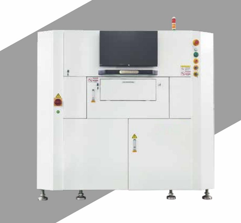
1200MM/1500MM Online SPI , Big Size Solder Paste Inspection Machine mail: sales@smtlinemachine.com whatapp/wechat:+8613537875415 Specification: 技术参数/Parameters 技术平台/Technology Platform super big size platform 适用
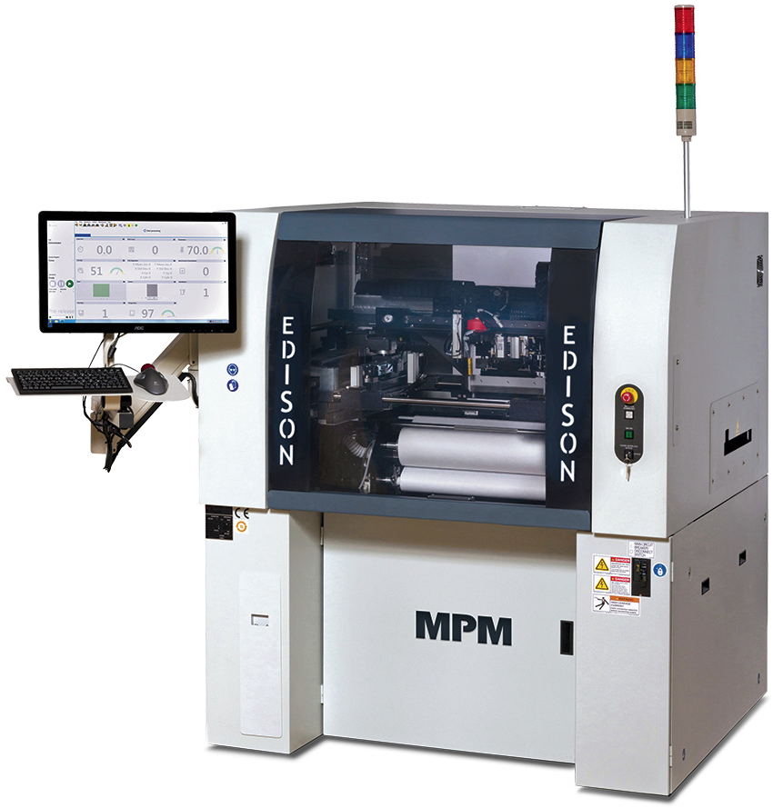
Unparalleled throughput and accuracy in an advanced next generation scalable printer platform. The MPM Edison™ stencil printer is ideally suited for the growing Automotive and Smart Device manufacturing markets. The Edison printer i
Electronics Forum | Fri May 21 15:50:41 EDT 1999 | John Thorup
We are running a number of boards with 8-10 25 mil PQFPs on board. Our process is mature with at least 3 years experiance and statistically few opens on the QFPs. Our beloved purchasing department has chased the almighty $ and changed FAB vendors
Electronics Forum | Mon May 24 13:33:46 EDT 1999 | Dave F
| We are running a number of boards with 8-10 25 mil PQFPs on board. Our process is mature with at least 3 years experiance and statistically few opens on the QFPs. Our beloved purchasing department has chased the almighty $ and changed FAB vendor
Used SMT Equipment | SPI / Solder Paste Inspection
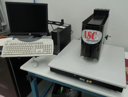
ASC International LaserVision SP3D-ADC - 3D Solder Paste Inspection - Benchtop - Model: SP3D-ADC - Automatic Data Collection (ADC) for real-time control of SMT stencil printing - 3D Profiling Capabilities - Windows® XP interface Operating Sy
Used SMT Equipment | SPI / Solder Paste Inspection
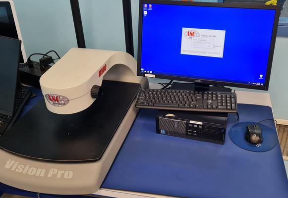
ASC VisionPro M500 3D Solder Paste Inspection System (2019) Brand: ASC InternationalModel: M500 3D Solder Paste Inspection SystemS/N: PSI-107Year: 2019Software: ASCan ULTRA Version 2.4.4.5O/S: Windows 10 Pro System SpecificationsMaximum Object Thickn
Industry News | 2014-01-17 12:52:25.0
BEST Inc., has developed a line of Kapton™ SMT stencils for the prototype assembly market. These stencils, available in 4,5 and 6 thicknesses, present very flat coplanar printing surfaces for solder paste printing. . They are designed to be used when the there are very few boards to be made at one time and the pitch of the components is 1.00 and above.
Industry News | 2015-12-04 13:06:33.0
December 3, 2015 – Continuing to invest in the most advanced stencil production technologies, FCT Assembly’s Fine Line Stencil division today announced that it has added a next-generation micro-milling system to its operation to enable production of highly-accurate step -- or multi-level -- stencils.
Technical Library | 2023-07-25 16:50:02.0
Some of the new handheld communication devices offer real challenges to the paste printing process. Normally, there are very small devices like 01005 chip components as well as 0.3 mm pitch uBGA along with other devices that require higher deposits of solder paste. Surface mount connectors or RF shields with coplanarity issues fall into this category. Aperture sizes for the small devices require a stencil thickness in the 50 to 75 um (2-3 mils) range for effective paste transfer whereas the RF shield and SMT connector would like at least 150 um (6 mils) paste height. Spacing is too small to use normal step stencils. This paper will explore a different type of step stencil for this application; a "Two-Print Stencil Process" step stencil. Here is a brief description of a "Two-Print Stencil Process". A 50 to 75 um (2-3 mils) stencil is used to print solder paste for the 01005, 0.3 mm pitch uBGA and other fine pitch components. While this paste is still wet a second in-line stencil printer is used to print all other components using a second thicker stencil. This second stencil has relief pockets on the contact side of the stencil any paste was printed with the first stencil. Design guidelines for minimum keep-out distances between the relief step, the fine pitch apertures, and the RF Shields apertures as well relief pocket height clearance of the paste printed by the first print stencil will be provided.
Technical Library | 2023-07-25 16:42:54.0
Printing solder paste for very small components like .3mm pitch CSP's and 01005 Chip Components is a challenge for the printing process when other larger components like RF shields, SMT Connectors, and large chip or resistor components are also present on the PCB. The smaller components require a stencil thickness typically of 3 mils (75u) to keep the Area Ratio greater than .55 for good paste transfer efficiency. The larger components require either more solder paste height or volume, thus a stencil thickness in the range of 4 to 5 mils (100 to 125u). This paper will explore two stencil solutions to solve this dilemma. The first is a "Two Print Stencil" option where the small component apertures are printed with a thin stencil and the larger components with a thicker stencil with relief pockets for the first print. Successful prints with Keep-Outs as small as 15 mils (400u) will be demonstrated. The second solution is a stencil technology that will provide good paste transfer efficiency for Area Ratio's below .5. In this case a thicker stencil can be utilized to print all components. Paste transfer results for several different stencil types including Laser-Cut Fine Grain stainless steel, Laser-Cut stainless steel with and w/o PTFE Teflon coating, AMTX E-FAB with and w/o PTFE coating for Area Ratios ranging from .4 up to .69.

1200MM/1500MM Online SPI , Big Size Solder Paste Inspection Machine mail: sales@smtlinemachine.com whatapp/wechat:+8613537875415 Specification: 技术参数/Parameters 技术平台/Technology Platform super big size platform 适用
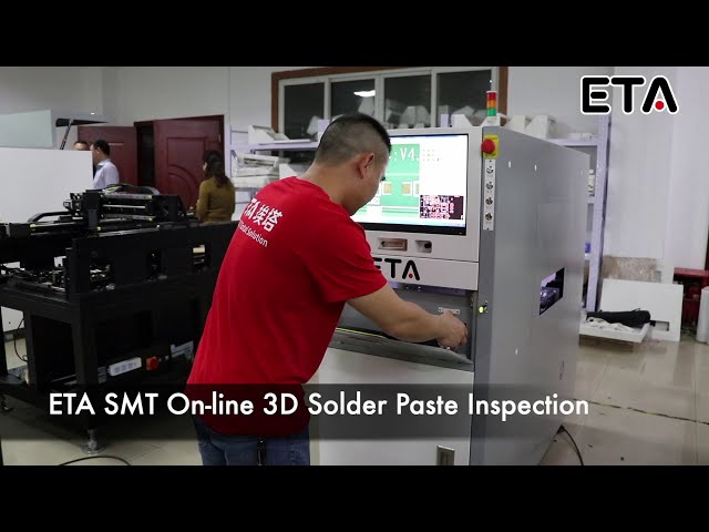
SMT On-line 3D Solder Paste Inspection If you could not find any similar items you want, you may send some photos to us. because our catalog and website haven't included all of our products. solder paste inspection,SMT SPI,SPI machine, SPI in
Career Center | , | Engineering,Production
Project Management, SMT Process Engineering
Career Center | Phoenix, Arizona | Engineering,Management,Production,Quality Control,Research and Development,Sales/Marketing,Technical Support
• Highly motivated, solution oriented professional with proven record synergizing scientific, engineering, and business administration backgrounds to drive and sustain customer satisfaction and long term improvements. • Articulate communicator that a
SMT Express, Volume 2, Issue No. 3 - from SMTnet.com Volume 2, Issue No. 3 Thursday, March 16, 2000 Featured Article Return to Front Page Stencil Design for Mixed Technology Through-hole / SMT Placement and Reflow by William E. Coleman, Photo
INSERT INTO tracking_express (userid, username, page_id, ts) VALUES ('#Quser_profile.id#', '#Quser_profile.username#', 36, (#ts#)) SMT Express, Volume 2, Issue No. 12 - from SMTnet.com Volume 2, Issue No. 12 Friday, December 15, 2000
PCB Libraries, Inc. | https://www.pcblibraries.com/Forum/when-should-a-pad-use-windowpane-paste-mask_topic2600_post10599.html
. Let's say you use a 0.125 mm (5 mil) stencil thickness. If you have a thermal pad that has 100% paste mask coverage, there is no where for the solder to flow and the package ends up sitting on top of
| http://etasmt.com/te_news_bulletin/2020-04-23/15761.chtml
. Soldering temperature curve: According to factors such as the number and thickness of the multilayer board of the PCB, the volume and density of the soldered components, the area and thickness of the copper layer on the PCB, etc


