New Equipment | Assembly Services
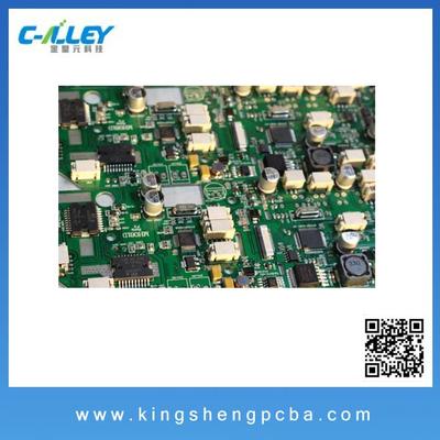
Our Service PCB Assembly and PCB&PCBA design are our main business.We are able to undertake a high quality Printed Circuit Board Assembly on competitive prices and flexible conditions.We are a complete “One- Stop” resource for printed circuit board
New Equipment | Fabrication Services
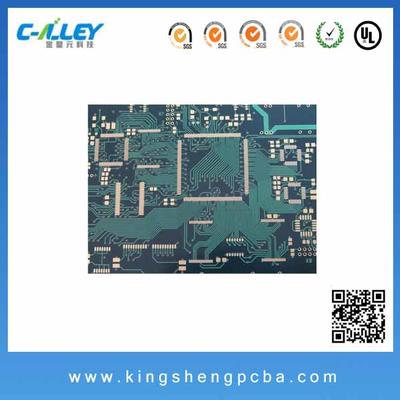
Our Service PCB Assembly and PCB&PCBA design are our main business.We are able to undertake a high quality Printed Circuit Board Assembly on competitive prices and flexible conditions.We are a complete “One- Stop” resource for printed circuit board
Electronics Forum | Mon May 07 11:02:17 EDT 2001 | Singh
Hi all. I am looking into the implementation of the Chip on Board process with eutactic bonding and the then using either gold or aluminum wire to make wedge type wire bonding. Since I am totally new to this, can somebody guide me thru the process,
Electronics Forum | Tue Jun 04 19:33:16 EDT 2002 | rob_thomas
Dave's estimation is pretty conservative but there is a lot of equipment out there and a lot of people happy to make a sale.Implementing both mentioned processes it's difficult and time consuming .Even if you get good training from whoever sells you
Industry News | 2003-03-11 08:45:00.0
CAMtastic DXP is the latest version of Altium's complete CAM verification and editing system that bridges the gap between PCB design and manufacturing and facilitates communication between board designers, fabrication engineers, and their clients.
Industry News | 2011-09-06 15:20:36.0
SMTA China announced the Best Paper/Presentation and Best Exhibit Awards at its annual awards presentation held in conjunction with SMTA China and Hong Kong Chapter Breakfast Reception, which took place August 31, 2011 at the Ritz-Carlton Hotel in Shenzhen.
Technical Library | 2016-08-24 06:15:35.0
From consumer electronics to systems control, automotive technology to aviation and aerospace – today, electronics are absolutely essential in many sectors. They increasingly replace mechanical components, eliminating wear and tear and thereby extending the service life. What is easily forgotten in this regard is that electronics are also subject to the laws of mechanics. Mechanical test equipment is crucial to test components for the secure hold of welded, soldered or adhesive bonds. A new, mechanically intricate test probe with universal clamping jaws, that can even grasp the individual bonding wires, is in line with the trend toward ever smaller components. Serving as an actuator for these is a micro drive that can be precisely controlled using a miniaturised motion controller to relieve the control unit in the test device.
Technical Library | 2020-08-27 01:22:45.0
Initially adopted internal specifications for acceptance of printed circuit boards (PCBs) used for wire bonding was that there were no nodules or scratches allowed on the wirebond pads when inspected under 20X magnification. The nodules and scratches were not defined by measurable dimensions and were considered to be unacceptable if there was any sign of a visual blemish on wire-bondable features. Analysis of the yield at a PCB manufacturer monitored monthly for over two years indicated that the target yield could not be achieved, and the main reasons for yield loss were due to nodules and scratches on the wirebonding pads. The PCB manufacturer attempted to eliminate nodules and scratches. First, a light-scrubbing step was added after electroless copper plating to remove any co-deposited fine particles that acted as a seed for nodules at the time of copper plating. Then, the electrolytic copper plating tank was emptied, fully cleaned, and filtered to eliminate the possibility of co-deposited particles in the electroplating process. Both actions greatly reduced the density of the nodules but did not fully eliminate them. Even though there was only one nodule on any wire-bonding pad, the board was still considered a reject. To reduce scratches on wirebonding pads, the PCB manufacturer utilized foam trays after routing the boards so that they did not make direct contact with other boards. This action significantly reduced the scratches on wire-bonding pads, even though some isolated scratches still appeared from time to time, which caused the boards to be rejected. Even with these significant improvements, the target yield remained unachievable. Another approach was then taken to consider if wire bonding could be successfully performed over nodules and scratches and if there was a dimensional threshold where wire bonding could be successful. A gold ball bonding process called either stand-off-stitch bonding (SSB) or ball-stitch-on-ball bonding (BSOB) was used to determine the effects of nodules and scratches on wire bonds. The dimension of nodules, including height, and the size of scratches, including width, were measured before wire bonding. Wire bonding was then performed directly on various sizes of nodules and scratches on the bonding pad, and the evaluation of wire bonds was conducted using wire pull tests before and after reliability testing. Based on the results of the wire-bonding evaluation, the internal specification for nodules and scratches for wirebondable PCBs was modified to allow nodules and scratches with a certain height and a width limitation compared to initially adopted internal specifications of no nodules and no scratches. Such an approach resulted in improved yield at the PCB manufacturer.
The FINEPLACER® Lambda, a modularly designed bonder, provides a full range of process capabilities and multiple bonding technologies. Read more: http://eu.finetech.de/micro-assembly/products/fineplacerr-lambda.html
With the development of miniaturization of assembly components, the layout area and pattern design area of PCBs have also been continuously reduced, and PCB manufacturers are constantly updating the production process to conform to the development tr
Gold Wire Bonding Performance and Reliability of ENEPIG Surface Finishes Gold Wire Bonding Performance and Reliability of ENEPIG Surface Finishes The expression "multifunctional PCB", as a synonym for a PCB which is applicable with a variety
SMT Express, Volume 2, Issue No. 9 - from SMTnet.com Volume 2, Issue No. 9 Thursday, September 14, 2000 Featured Article Return to Front Page Book Review Reviewed by Dave Fish (davef ), Pandion Electronics, Inc Title: Wire Bonding
| https://www.eptac.com/ask/training-in-wire-bonding/
Training in Wire Bonding - EPTAC - Train. Work Smarter. Succeed Looking for solder training standards, manuals, kits, and more
ASYMTEK Products | Nordson Electronics Solutions | https://www.nordson.com/en/divisions/adhesive-dispensing-systems/industries/construction-and-architectural/cable-manufacturing?con=t&page=6
Nordson hot and cold material dispensing or powder coating for wire and cable manufacturing Adhesive Dispensing Systems Corporate | Global Directory


