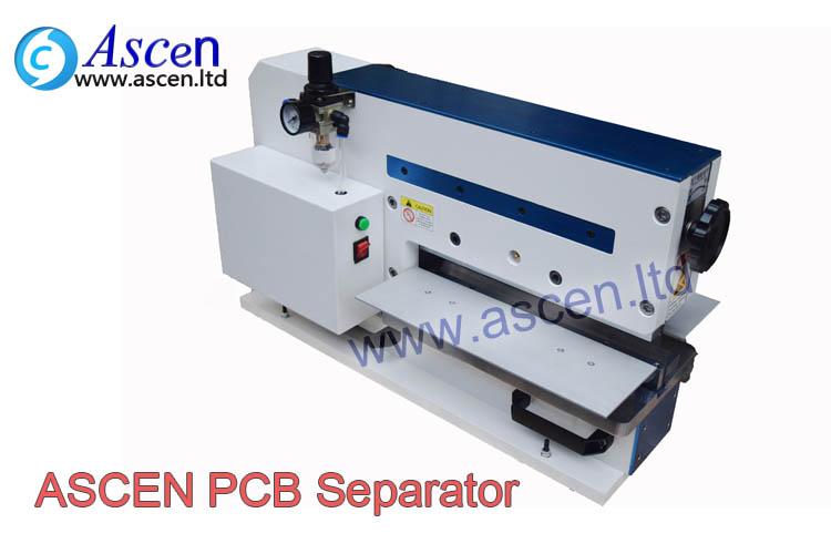
ASCEN PCB cutting machine ASC-620 model can separate PCB board with high component placed close to the edge can be separated safety, with minimum internal stress, especially suitable to separation of precise SMD or thin board. Unlike double roun
Henkel offers innovative capillary flow underfill encapsulants for flip-chip, CSP and BGA devices. These are highly flowable, high purity, onecomponent encapsulants. They form a uniform and void-free underfill layer to improve reliability performance
Electronics Forum | Thu Dec 26 12:12:55 EST 2013 | igorfo
Dear Friends, I need your help to understand requirements and measurement methods for bow and twist of assembled PCB (PCBA have and SMT and TH components). I already check all posts on the site but didn't found any related to my question answers.
Electronics Forum | Wed Aug 19 08:00:55 EDT 1998 | Earl Moon
| Hi there, | I'm actually facing a lot of trouble with PCB's presenting up to 3mm of bow /twist at reception i.e. before assembly. The PCB size is 220 by 230mm. The boards are to be assembeled SMD double sides with 05.mm pitch on both sides. In orde
Industry News | 2017-05-10 18:15:53.0
Nordson ASYMTEK and Nordson MARCH, Nordson companies (NASDAQ: NDSN), will present papers at the Conformal Coating Materials and Processes session at the Contamination, Cleaning, and Coating Conference being held in Amsterdam, Netherlands. Transitioning from Manual to Automated Conformal Coating, by Michael Szuch, Nordson ASYMTEK and Optimizing the Plasma Treatment Process Prior to Conformal Coating to Eliminate ESD Induced Failures, by David Foote, Nordson MARCH, will be presented on Wednesday, May 24, 2017.
Industry News | 2009-02-21 17:56:00.0
BANNOCKBURN, Ill. and ARLINGTON, Va., USA, February 19, 2009 � IPC � Meeting the requirements of RoHS (restriction of the use of certain hazardous substances in electrical and electronic equipment) compliance and successfully implementing lead-free electronics assembly processes is an ongoing challenge for the electronic interconnect industry. To help companies work toward their compliance goals, IPC and JEDEC present �Transitioning to Lead Free � Strategies for Implementation,� a three-day conference to be held March 3�5, 2009 in Santa Clara, Calif.
Technical Library | 2023-02-13 18:56:42.0
This paper describes the results of an intensive whisker formation study on Pb-free assemblies with different levels of cleanliness. Thirteen types of as-received surface-mount and pin-through-hole components were cleaned and intentionally contaminated with solutions containing chloride, sulfate, bromide, and nitrate. Then the parts were assembled on double-sided boards that were also cleaned or intentionally contaminated with three fluxes having different halide contents. The assemblies were subjected to high-temperature/high-humidity testing (85_C/85% RH). Periodic examination found that contamination triggered whisker formation on both exposed tin and solder fillets. Whisker occurrence and parameters depending on the type and level of contamination are discussed. Cross-sections were used to assess the metallurgical aspects of whisker formation and the microstructural changes occurring during corrosion.
Events Calendar | Wed Jun 19 00:00:00 EDT 2019 - Sat Jun 22 00:00:00 EDT 2019 | Bangkok, Thailand
NEPCON Thailand - Assembly, Measurement and Testing Technologies for Electronics Manufacturing Expo
Imagineering, Inc. | https://www.pcbnet.com/blog/hdi-pcb-advantages-and-applications/
. This type of PCB technology allows for improved functionality in smaller consumer products, denser BGA and QFP packages, and lowered heat transfer induced stress
Heller Industries Inc. | https://hellerindustries.com/wp-content/uploads/2018/07/last-will-of-bga-void.pdf
. Figure 29 and Figure 30 illustrate the defective U1 component pad location. The solder joint has a pad impression where it made electrical contact before the thermal cycle induced stresses caused failure. Figure 29. Macro View, BGA56 U1 Component Cross


