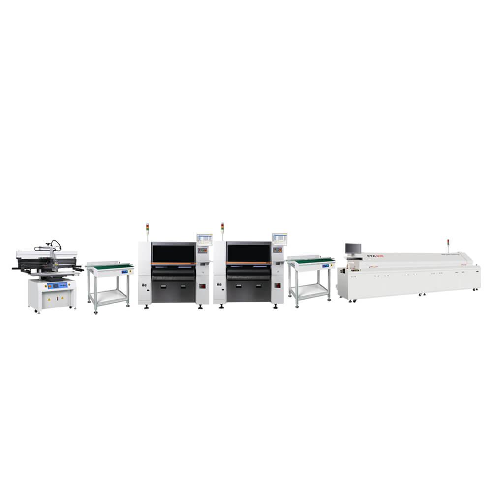
LED Assembly Line/ SMT Assembly Line/ PCBA Line (printer+mounter+reflow oven) Name: SMT assembly line Usage: PCB production Type: Semi auto Production time: 30 days Product description: LED Assembly Line/ SMT Assembly Line/ PCBA Line (printer+

China SMT Assembly Line Total Solution factory Manufacturer Name: SMT assembly line Usage: PCB production Type: Semi auto Production time: 30 days Product description: China SMT Assembly Line Total Solution factory Manufacturer INQUIR
Electronics Forum | Mon Jan 12 21:31:26 EST 2015 | warwolf
The closer your inspection the more defects you will find, the more rework you do the possible cost you will add and the potential increase of damage you could do to your products if rework is not up to a machine copyable standard. "Is there any in
Electronics Forum | Fri Apr 17 14:03:48 EDT 1998 | Earl Moon
| Hello Ya'll, | I've got what may be a silly question, but why does it seem so important to everybody that you have x-ray capability if you're thinking about doing BGA? | I know what most people will tell me; "Steve, that's a pretty silly qu
Industry News | 2012-01-23 00:02:12.0
MIRTEC, “The Global Leader in Inspection Technology”, will premier its complete line of 3D AOI, SPI, X-ray and LED inspection systems at the IPC APEX Expo in booth #3637.
Industry News | 2010-08-04 21:04:22.0
Manufacturing reliable and sustainable electronics that meet customer needs without failure during the product’s life cycle has been stymied by myriad challenges, from environmental regulations to new materials and processes. Bringing together the latest research by industry experts, IPC — Association Connecting Electronics Industries® will host a Technical Conference on Electronics Sustainability, September 28–30 at Electronics Midwest, in Rosemont, Ill. Electronics Midwest is produced jointly by IPC and Canon Communications.
Technical Library | 2012-12-14 14:28:20.0
This paper examines the potential failure mechanisms that can damage modern lowvoltage CMOS devices and their relationship to electrical testing. Failure mechanisms such as electrostatic discharge (ESD), CMOS latch-up, and transistor gate oxide degradation can occur as a result of electrical over-voltage stress (EOS). In this paper, EOS due to electrical testing is examined and an experiment is conducted using pulsed voltage waveforms corresponding to conditions encountered during in-circuit electrical testing. Experimental results indicate a correlation between amplitude and duration of the pulse waveform and device degradation due to one or more of the failure mechanisms.
Technical Library | 2016-05-19 16:03:37.0
As consumers become more reliant on their handheld electronic devices and take them into new environments, devices are increasingly exposed to situations that can cause failure. In response, the electronics industry is making these devices more resistant to environmental exposures. Printed circuit board assemblies, handheld devices and wearables can benefit from a protective conformal coating to minimize device failures by providing a barrier to environmental exposure and contamination. Traditional conformal coatings can be applied very thick and often require thermal or UV curing steps that add extra cost and processing time compared to alternative technologies. These coatings, due to their thickness, commonly require time and effort to mask connectors in order to permit electrical conductivity. Ultra-thin fluorochemical coatings, however, can provide excellent protection, are thin enough to not necessarily require component masking and do not necessarily require curing. In this work, ultra-thin fluoropolymer coatings were tested by internal and industry approved test methods, such as IEC (ingress protection), IPC (conformal coating qualification), and ASTM (flowers-of-sulfur exposure), to determine whether this level of protection and process ease was possible.

· What is the difference between SMT vacuum reflow soldering machine and ordinary reflow soldering machine? · What problems can be solved by smt vacuum reflow soldering machine? · What is the basic principle of vacuum reflow machine? · Ho
SMTnet Express, June 19, 2014, Subscribers: 22851, Members: Companies: 13906, Users: 36363 Anisotropic grain growth and crack propagation in eutectic microstructure under cyclic temperature annealing in flip-chip SnPb composite solder joints Y
| https://www.smtfactory.com/Compared-with-Wave-Soldering-What-are-the-Features-and-Advantages-of-Lyra-Reflow-Oven-id3425979.html
only applies solder on the required parts, and can control the application amount. When the component placement position deviates to a certain extent, due to the surface tension of the molten solder, as long as the solder placement position is correct, the reflow soldering can
ASYMTEK Products | Nordson Electronics Solutions | https://www.nordson.com/en/divisions/dage/technical-experts/micro-testing-thin-die
. These flaws manifest themselves as chips and scratches. Die can experience high levels of stress due to CTE mismatch or flexure of the substrate or board that they are mounted to

.gif)


