New Equipment | Solder Materials
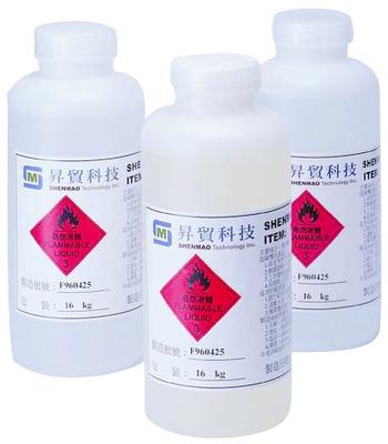
We offer a full line of Water Soluble Fluxes and No-Clean Flux for SMT, IC packaging and PCB Wave solder applications. We provide halide-containing and halide-free fluxes for Lead-Free solder alloys. Besides, our Lead-Free Liquid Fluxes have been a
Hitachi SIGMA F8 Pick and Place Machine Hitachi SIGMA F8 Pick and Place Machine Hitachi SIGMA F8 Mounting Speed:156,000CPH Applicable components: 0402 Product description: Hitachi SIGMA F8 Pick and Place Machine, Mounting Speed:156,000CPH, Appl
Industry News | 2011-02-24 20:35:03.0
The SMTA is pleased to announce the program for the 2011 International Conference on Soldering and Reliability being held May 3-6 in Toronto, Ontario, Canada.
Industry News | 2022-02-07 17:22:07.0
The electronics manufacturing industry is applauding a bill being voted on this week in the U.S. House of Representatives, which would, if enacted, launch a new era of federal government partnership with the industry.

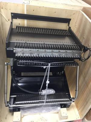
Parts & Supplies | Pick and Place/Feeders
Detailed Product Description we provide SMT kinds of feeders, Main business are CM402,CM602,CM101,NPM,BM, YAMAHA....etc., Original new and used both have , we wish establishing long-term cooperations , welcome to contact ,thanks! Item Model Part
Parts & Supplies | Pick and Place/Feeders
Detailed Product Description Our company supply SMT equipment original new parts, such as: CM402/602/202/NPM, Best price with Best Quality , is willing to establish long-term friendly relations of cooperation, welcome to contact us! N610064416AA
Technical Library | 2021-06-21 19:34:02.0
In this era of electronics miniaturization, high yield and low-cost integrated circuit (IC) substrates play a crucial role by providing a reliable method of high density interconnection of chip to board. In order to maximize substrate real-estate, the distance between Cu traces also known as line and space (L/S) should be minimized. Typical PCB technology consists of L/S larger than 40 µ whereas more advanced wafer level technology currently sits at or around 2 µm L/S. In the past decade, the chip size has decreased significantly along with the L/S on the substrate. The decreasing chip scales and smaller L/S distances has created unique challenges for both printed circuit board (PCB) industry and the semiconductor industry. Fan-out panel-level packaging (FOPLP) is a new manufacturing technology that seeks to bring the PCB world and IC/semiconductor world even closer. While FOPLP is still an emerging technology, the amount of high-volume production in this market space provide a financial incentive to develop innovative solutions in order to enable its ramp up. The most important performance aspect of the fine line plating in this market space is plating uniformity or planarity. Plating uniformity, trace/via top planarity, which measures how flat the top of the traces and vias are a few major features. This is especially important in multilayer processing, as nonuniformity on a lower layer can be transferred to successive layers, disrupting the device design with catastrophic consequences such as short circuits. Additionally, a non-planar surface could also result in signal transmission loss by distortion of the connecting points, like vias and traces. Therefore, plating solutions that provide a uniform, planar profile without any special post treatment are quite desirable.
Today's Hot Deals: DR331-513AE 61300211121 BTT6010-1ERA BTT60101ERAXUMA1 ATXMEGA32A4U-AU TPA3129D2DAPR BCM85110IFSBG IRS2093MTRPBF SN74LV595ARGYRG4 TJA1043TK/1Y ATTINY861A-SU CZWH-32-S XC7A50T-1FGG484 XC7A100T-1FGG484 TPS7B7702QPWPRQ1
Today's Hot Deals: DR331-513AE 61300211121 BTT6010-1ERA BTT60101ERAXUMA1 ATXMEGA32A4U-AU TPA3129D2DAPR BCM85110IFSBG IRS2093MTRPBF SN74LV595ARGYRG4 TJA1043TK/1Y ATTINY861A-SU CZWH-32-S XC7A50T-1FGG484 XC7A100T-1FGG484 TPS7B7702QPWPRQ1


