1.jpg)
New Equipment | Industrial Automation
Sandy.[mailto:unity@mvme.cn] Sandy.[WhatsApp/Skype/Mobile:+8618020776786] Sandy.[Quote to you within the shortest possible time with our best price] Warranty: up to 12 months Shipping: fast delivery is available NEW+ORIGINAL+IN STOCK+ONE
1.jpg)
New Equipment | Industrial Automation
Sandy.[mailto:unity@mvme.cn] Sandy.[WhatsApp/Skype/Mobile:+8618020776786] Sandy.[Quote to you within the shortest possible time with our best price] Warranty: up to 12 months Shipping: fast delivery is available NEW+ORIGINAL+IN STOCK+ONE
Electronics Forum | Wed Jun 26 22:05:35 EDT 2019 | SMTA-Chi Hong
Hello all, Recently there is component SOIC8L HD leadframe with the exposed Cu on shoulder side and lead tip. Is anyone have experience running with this type of component?Thanks
Electronics Forum | Wed May 27 10:15:52 EDT 1998 | Doug Romm
Just wanted to add a few comments on the discussion of how to identify palladium parts. Generally, there is no "clear-cut" way to identify Pd versus Sn/Pb. It mainly comes with experience. Any part that is is plated prior to being trim/formed will
Industry News | 2018-04-09 19:48:04.0
SMTA Europe announces Session 1 Technical Program on Predicting Component Life at the “Electronics in Harsh Environments Conference” to be held in Amsterdam, Netherlands, on April 25th, 2018.
Industry News | 2018-10-18 08:59:34.0
PRINCIPLE OF SURFACE MOUNT PROCESS(SMT PROCESS)
Technical Library | 2015-06-22 16:39:47.0
Surface finishing is an integral part of any PCB fabrication. It is generally applied to exposed Cu connectors and conductors on the board. Surface finishing has numerous important functions. It serves as a protective layer for the Cu connectors during storage. The surface finish helps minimize or reduce tarnish of the Cu substrate. Additionally, since it is the layer that comes into contact with other components during assembly, it ensures good solderability between the PCB and the component during assembly. Furthermore after assembly, the finish helps prolong the integrity of the solder joint during use. A general review of common PCB surface finishes is presented. The advantages and disadvantages of each are discussed and compared.
Technical Library | 2021-11-03 17:05:39.0
Additively printed circuits provide advantages in reduced waste, rapid prototyping, and versatile flexible substrate choices relative to conventional circuit printing. Copper (Cu) based inks along with intense pulsed light (IPL) sintering can be used in additive circuit printing. However, IPL sintered Cu typically suffer from poor solderability due to high roughness and porosity. To address this, hybrid Cu ink which consists of Cu precursor/nanoparticle was formulated to seed Cu species and fill voids in the sintered structure. Nickel (Ni) electroplating was utilized to further improve surface solderability. Simulations were performed at various electroplating conditions and Cu cathode surface roughness using the multi-physics finite element method. By utilizing a mask during IPL sintering, conductivity was induced in exposed regions; this was utilized to achieve selective Ni-electroplating. Surface morphology and cross section analysis of the electrodes were observed through scanning electron microscopy and a 3D optical profilometer. Energy dispersive X-ray spectroscopy analysis was conducted to investigate changes in surface compositions. ASTM D3359 adhesion testing was performed to examine the adhesion between the electrode and substrate. Solder-electrode shear tests were investigated with a tensile tester to observe the shear strength between solder and electrodes. By utilizing Cu precursors and novel multifaceted approach of IPL sintering, a robust and solderable Ni electroplated conductive Cu printed electrode was achieved.
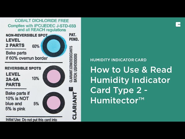
A Sustainable Alternative - Humitector cards are halogen-free and cobalt dichloride free. Visit https://www.clariant.com/solutions/products/2017/10/31/00/12/humitector-type-2-nonreversible-humidity-indicator-card?utm_source=CLRYouTube&utm_medium=Vi
SMTnet Express February 28, 2013, Subscribers: 26214, Members: Companies: 13305, Users: 34373 Effect of Cooling Rate on the Intermetallic Layer in Solder Joints While it has long been known that the Cu6Sn5 intermetallic that plays a critical role
applied to exposed Cu connectors and conductors on


