New Equipment | Solder Materials
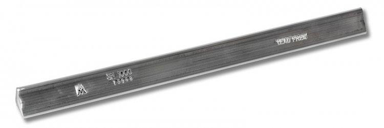
SN100C is a lead-free solder alloy developed by Nihon Superior in Japan that is comprised of tin-copper-nickel + germanium. SN100C offers user-friendly properties and has been proven in commercial production since 1999. The result of these advantages
1.Our Advantages 1.1. Japan Hamamatsu X-ray tube, the best closed type X-ray tube in the world, with the longest lifetime and maintenance-free. 1.2 New generation Korea Rayence HD digital flat panel detector (FPD), eliminate the image intensifier.
Electronics Forum | Fri Jun 22 07:16:37 EDT 2012 | brettrenishaw
Spray fluxing yes but have checked the uniformity by using a fluxometer. Also have put boards through with only flux and preheat. no wave up to see if the carrier is being burnt off. I will look into the skip plating issue. Thanks again
Electronics Forum | Tue Nov 07 22:44:39 EST 2017 | wrander1
Hi I'm new to the world of wire bonding. I seem to have some sort of pad contamination Preventing gold wire from bonding to aluminum pats. There appears to be a dozen microns size particles. And a slight crackling of the surface at 500 X. I am send
Industry News | 2011-08-18 21:23:09.0
For an industry that is constantly advancing, the technical conference at IPC Midwest Conference & Exhibition on September 21–22, in Schaumburg, Ill., will feature five sessions offering the latest research, methodologies and insights from industry experts to address critical challenges of manufacturing defect-free, quality electronics.
Industry News | 2011-08-18 21:24:08.0
For an industry that is constantly advancing, the technical conference at IPC Midwest Conference & Exhibition on September 21–22, in Schaumburg, Ill., will feature five sessions offering the latest research, methodologies and insights from industry experts to address critical challenges of manufacturing defect-free, quality electronics.
Technical Library | 2020-08-27 01:22:45.0
Initially adopted internal specifications for acceptance of printed circuit boards (PCBs) used for wire bonding was that there were no nodules or scratches allowed on the wirebond pads when inspected under 20X magnification. The nodules and scratches were not defined by measurable dimensions and were considered to be unacceptable if there was any sign of a visual blemish on wire-bondable features. Analysis of the yield at a PCB manufacturer monitored monthly for over two years indicated that the target yield could not be achieved, and the main reasons for yield loss were due to nodules and scratches on the wirebonding pads. The PCB manufacturer attempted to eliminate nodules and scratches. First, a light-scrubbing step was added after electroless copper plating to remove any co-deposited fine particles that acted as a seed for nodules at the time of copper plating. Then, the electrolytic copper plating tank was emptied, fully cleaned, and filtered to eliminate the possibility of co-deposited particles in the electroplating process. Both actions greatly reduced the density of the nodules but did not fully eliminate them. Even though there was only one nodule on any wire-bonding pad, the board was still considered a reject. To reduce scratches on wirebonding pads, the PCB manufacturer utilized foam trays after routing the boards so that they did not make direct contact with other boards. This action significantly reduced the scratches on wire-bonding pads, even though some isolated scratches still appeared from time to time, which caused the boards to be rejected. Even with these significant improvements, the target yield remained unachievable. Another approach was then taken to consider if wire bonding could be successfully performed over nodules and scratches and if there was a dimensional threshold where wire bonding could be successful. A gold ball bonding process called either stand-off-stitch bonding (SSB) or ball-stitch-on-ball bonding (BSOB) was used to determine the effects of nodules and scratches on wire bonds. The dimension of nodules, including height, and the size of scratches, including width, were measured before wire bonding. Wire bonding was then performed directly on various sizes of nodules and scratches on the bonding pad, and the evaluation of wire bonds was conducted using wire pull tests before and after reliability testing. Based on the results of the wire-bonding evaluation, the internal specification for nodules and scratches for wirebondable PCBs was modified to allow nodules and scratches with a certain height and a width limitation compared to initially adopted internal specifications of no nodules and no scratches. Such an approach resulted in improved yield at the PCB manufacturer.
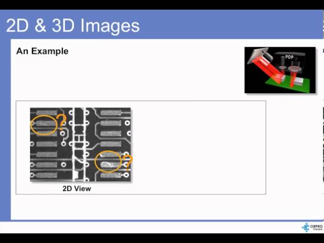
ORPRO Vision SPI Presentation. This presentation introduces the methods and technology used by ORPRO Vision in the Symbion P36 Plus SPI system. For additional information, please contact ORPRO Vision at sales.us@orprovision.com sales.eu@orprovision
Training Courses | | | PCB Rework and Hand Soldering Courses
The PCB rework and hand soldering courses courses cover techniques of rework and repair of PCBs, BGAs and other electronics assemblies, and teach fundamentals of soldering of electronics assemblies.
ASYMTEK Products | Nordson Electronics Solutions | https://www.nordson.com/en/divisions/efd/resource-center/solder-glossary-of-terms
. Some typical brazing alloys include copper-zinc, copper-gold, copper-phosphorous, and silver-based alloys. The melting temperatures for brazing alloys range from 450° C (852° F) to 1100° C (2012° F


