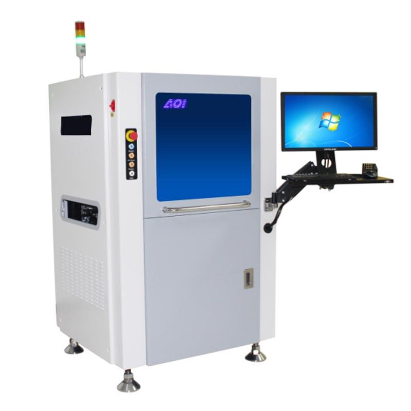
automated optical inspection AOI manufacturers in China keywords: AOI machine, AOI, automated optical inspection, AOI machine cost, AOI machine for PCB, SMT AOI machine, SMT AOI, SMD AOI, SMD AOI machine CATEGORY ITEM
Electronics Forum | Tue Jan 21 13:51:19 EST 2014 | rgduval
Armando, Is the problem in the same spot on the board with every run? If so, there might be something about that particular location that is part of the cause (ie. ground or power plane connection). It sounds like you're seeing blow holes, or insu
Electronics Forum | Wed Jan 15 21:55:41 EST 2014 | padawanlinuxero
we do that and there's a variation on the solder temp. sometimes around 10 degrees, we have 2 solder pallets that are run in intervals of roughly 3 1/2 minutes a part (the time that take the operator to put all 3 terminals in a 42 pcbs per board, and
Industry News | 2003-06-10 08:16:44.0
The following text describes the application of NWA Quality Analyst to quality control in the assembly of electronic components.
Industry News | 2023-01-23 18:11:48.0
MIRTEC Co. LTD, reports continued growth in Sales Revenue for its North American Sales and Service Division for 2022. "We are very pleased to announce that sales revenue for our North American Division has grown by over 22.6% with respect to 2021." stated Brian D'Amico, President of MIRTEC Corp.
Technical Library | 2008-03-18 12:36:31.0
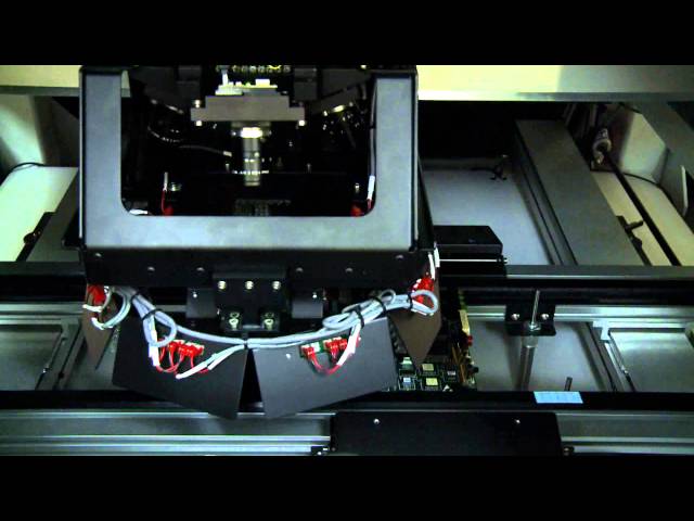
This paper examines the construction of a notebook mainboard with more than 2000 components and no wave soldering required. The board contains standard SMD, chipset BGAs, connectors, through hole components and odd forms placed using full automation and soldered after two reflow cycles under critical process parameters. However, state of the art technology does not help if the process parameters are not set carefully. Can all complex BGAs, THTs and even screws be soldered on a single stencil? What will help us overcome bridging, insufficient solder and thombstoning issues? This paper will demonstrate the placement of all odd shape components using pin-in-paste stencil design and full completion of the motherboard after two reflow cycles.
Technical Library | 2023-11-20 18:10:20.0
The electronics production is prone to a multitude of possible failures along the production process. Therefore, the manufacturing process of surface-mounted electronics devices (SMD) includes visual quality inspection processes for defect detection. The detection of certain error patterns like solder voids and head in pillow defects require radioscopic inspection. These high-end inspection machines, like the X-ray inspection, rely on static checking routines, programmed manually by the expert user of the machine, to verify the quality. The utilization of the implicit knowledge of domain expert(s), based on soldering guidelines, allows the evaluation of the quality. The distinctive dependence on the individual qualification significantly influences false call rates of the inbuilt computer vision routines. In this contribution, we present a novel framework for the automatic solder joint classification based on Convolutional Neural Networks (CNN), flexibly reclassifying insufficient X-ray inspection results. We utilize existing deep learning network architectures for a region of interest detection on 2D grayscale images. The comparison with product-related meta-data ensures the presence of relevant areas and results in a subsequent classification based on a CNN. Subsequent data augmentation ensures sufficient input features. The results indicate a significant reduction of the false call rate compared to commercial X-ray machines, combined with reduced product-related optimization iterations.
500,000 components per hour Maximum Board Size: 22” x 20” (560mm x 510mm) Clearance: 2” (50mm) top and bottom Minimum Component Size: 0201; 01005 with high magnification option
| https://www.eptac.com/faqs/soldertips/soldertip/soldertip-36-wave-soldering-insufficient-fill-and-voids-in-pth
SolderTip #36: Wave Soldering Insufficient Fill and Voids in PTH - EPTAC - Train. Work Smarter. Succeed Looking for solder training standards, manuals, kits, and more
PCB Libraries, Inc. | https://www.pcblibraries.com/Forum/smt-headers_topic736.html
: 20 Mar 2012 Location: Oxfordshire, UK Status: Offline Points: 576 Post Options Post Reply Quote jameshead Report Post Thanks(0) Quote Reply Topic: SMT Headers Posted: 23 Jan 2013 at 2:21am Thanks Tom, I only did this in this one case to find out what pad styles would be needed to be added to a technology file


