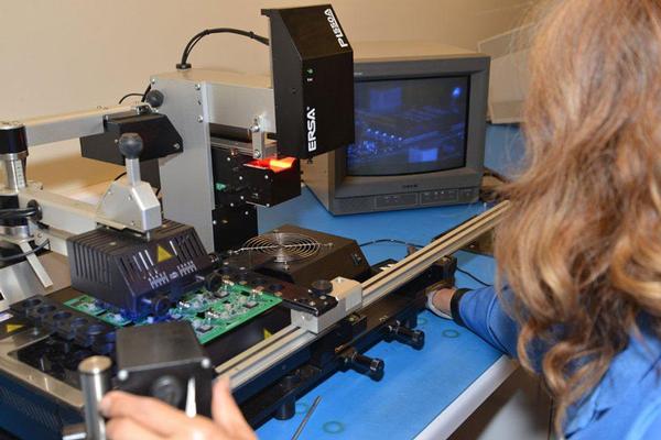
New Equipment | Rework & Repair Services
STI has qualified technicians trained in IPC 7711/7721, as well as in custom design solutions, to address your electronic rework and repair needs. STI’s services encompass both mainstream assembly technologies (surface mount and through-hole) as well
New Equipment | Rework & Repair Services
BGA and QFN removal, replacement & re-balling services ECO rework services – jumper wires, etch cuts, etc. Component and Memory Upgrades Trace and Pad repair Revision Updates Quick-turn ECO rework capabilities
Electronics Forum | Fri May 22 08:04:30 EDT 2009 | stevezeva
Have any of you ever worked with Actel's QFN 180? A three row I/O QFN? Actel has a published paper on design and assembly guidelines, but we're finding that they are pretty much generic, and don't really work as well as they lead you to believe. ht
Electronics Forum | Tue Jun 25 01:24:25 EDT 2019 | sssamw
That is possibley CTE mismatch between QFN and PCB material, the thicker PCB the higher fail rate.
Industry News | 2016-04-06 12:45:01.0
The SMTA is excited to announce three new workshops for the 10th Annual International Conference on Soldering and Reliability (ICSR) being held May 9-11, 2016 in Toronto, Canada. The event is co-located with the SMTA Toronto Expo.
Technical Library | 2015-06-11 21:20:29.0
The use of bottom terminated components (BTC) has become widespread, specifically the use of Quad Flat No-lead (QFN) packages. The small outline and low height of this package type, improved electrical and thermal performance relative to older packaging technology, and low cost make the QFN/BTC attractive for many applications.Over the past 15 years, the implementation of the QFN/BTC package has garnered a great amount of attention due to the assembly and inspection process challenges associated with the package. The difference in solder application parameters between the center pad and the perimeter pads complicates stencil design, and must be given special attention to balance the dissimilar requirements
Technical Library | 2012-10-18 21:58:51.0
First published in the 2012 IPC APEX EXPO technical conference proceedings. In this paper, we report on a comprehensive study regarding the morphology evolution and voiding of SnAgCu solder joints on the central pad of two different packages – QFN and an Agilent package called TOPS – on PCBs with a Ni/Au surface finish.
LISA SPIDER robot pick and place machine 2D/3D vision components copanarity check Tape & reel for tape OUT process Tray stacker for Tray IN proce/OUT process Tape IN feeder Anyfeeder for loose component sorting More under www.aatec.ch
TI New and Original TPS25940ARVCR in Stock QFN20 package TI New and Original TPS25940ARVCR in Stock QFN20 package TI New and Original TPS25940ARVCR in Stock QFN20 package LM27313XMF NS LM2904 NS LM2904DR NS LM2937IMP-3.3 NS LM2937IMP-5.0 NS
Minimizing Voiding In QFN Packages Using Solder Preforms SMTnet Express July 27, 2012, Subscribers: 25333, Members: Companies: 8933, Users: 33366 Minimizing Voiding In QFN Packages Using Solder Preforms First published in the 2012 IPC APEX EXPO
The Morphology Evolution and Voiding of Solder Joints on QFN Central Pads with a Ni/Au Finish SMTnet Express October 19, 2012, Subscribers: 25598, Members: Companies: 9011, Users: 33828 The Morphology Evolution and Voiding of Solder Joints on QFN
PCB Libraries, Inc. | https://www.pcblibraries.com/forum/qfn-dual-row_topic1032_post3976.html
: 16 May 2012 Location: San Diego Status: Offline Points: 423 Post Options Post Reply Quote Jeff.M Report Post Thanks(0) Quote Reply Topic: QFN Dual Row Posted: 22 Jul 2013 at 9:54am There is already and option to make dual row QFN's it's just not among the standard QFN family of parts
ASYMTEK Products | Nordson Electronics Solutions | https://www.nordson.com/en/divisions/dage/applications/test-and-inspection
. Detect a wide range of manufacturing defects including BGA, QFN and IGBT attachment, PTH filling, interfacial voiding, component cracking


