Industry Directory | Distributor / Manufacturer
AllPoint Electronics is specialized in SMT, PTH, and TEST Equipment and services for electronics industry in Brazilian market. We provide full support for PCB assembly factory implementation, and process consulting
Industry Directory | Consultant / Service Provider / Manufacturer
Lepla srl electronic contract manufacturer, specialized in the SMT & THT Electronic Cards Assembling, Wiring Assembling Harness, In-Circuit, Parametric and Functional Testing.
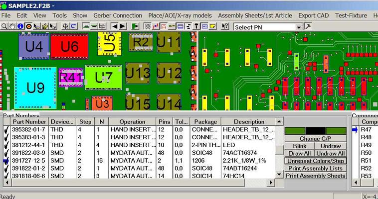
ProntoVIEW-MARKUP is assembly CAD Viewer & Gerber Viewer software used by electronics manufacturers to quickly find components, pin, shorts between traces, etc. ProntoVIEW-MARKUP is also a redline tool that allows annotation of the assembly to creat

The PCB Footprint Expert is a powerful CAD library development tool powered by our own proprietary CAD LEAP Technology (Libraries Enhanced with Automated Preferences). It is packed with very powerful advanced library management features that cuts foo
Electronics Forum | Wed Apr 08 11:30:03 EDT 1998 | mpark
Clint, You may want to call KJ Marketing Services, a Canadian company that fabricates plastic laser cut stencil. They call it "Kepoch stencil" This material was originally developed by Dupont, and patented and marketed by KJ. It was available for
Electronics Forum | Thu Nov 18 10:56:16 EST 1999 | Dave F
Jacky: There�re major four factors that affect the reliability of a solder connection. 1 Design of the connection including the shape and height of the lead and the type and amount of solder. 2 Dissolution of base metals into the solder connection.
Used SMT Equipment | Screen Printers
Substrate processing: Maximum substrate size (XxY): 609.6mmx508mm(24”x20”) For circuit boards larger than 20”, special fixtures are required Minimum substrate size (XxY): 50.8mmx50.8mm(2”x2”)
Used SMT Equipment | Pick and Place/Feeders
Product Details of 3D SPI-6500 Thick Paste Measurement Instrument Product Functions 1, friendly programming interface 2, a variety of measurement methods 3, scan spacing adjustable 4, image 3D simulation function 5, independent 3D dynamic obser
Industry News | 2021-12-09 09:26:46.0
Baja Bid is liquidating excess equipment via online auction. The bidding for this event is now open and the closing will begin today at 1:00 pm EST.
Industry News | 2018-10-18 11:18:14.0
Making Readable Silkscreen Layouts for your Printed Circuit Board (PCB) Design
Parts & Supplies | Pick and Place/Feeders
SMT basic process components include: silk screen (or dispensing), placement (curing), reflow soldering, cleaning, testing, repair 1, silk screen: its role is to paste or patch solder paste printed on the PCB pad, the components f

Parts & Supplies | SPI / Solder Paste Inspection
Quick programming, friendly programming interface Multiple measurement methods True one-button measurement Eight-way motion button, one-click focus Adjustable scanning pitch Solder paste 3D simulation function Powerful SPC function MARK
Technical Library | 2016-11-30 15:53:15.0
The use of microvias in Printed Circuit Boards (PCBs) for military hardware is increasing as technology drives us toward smaller pitches and denser circuitry. Along with the changes in technology, the industry has changed and captive manufacturing lines are few and far between. As PCBs get more complicated, the testing we perform to verify the material was manufactured to our requirements before they are used in an assembly needs to be reviewed to ensure that it is sufficient for the technology and meets industry needs to better screen for long-term reliability. The Interconnect Stress Testing (IST) protocol currently used to identify manufacturing issues in plated through holes, blind, or buried vias are not necessarily sufficient to identify problems with microvias. There is a need to review the current IST protocol to determine if it is adequate for finding bad microvias or if there is a more reliable test that will screen out manufacturing inconsistencies. The objective of this research is to analyze a large population of PCB IST coupons to determine if there is a more effective IST test to find less reliable microvias in electrically passing PCB product and to screen for manufacturing deficiencies. The proposed IST test procedure will be supported with visual inspection of corresponding microvia cross sections and Printed Wiring Assembly (PWA) acceptance test results. The proposed screening will be shown to only slightly affect PCB yield while showing a large benefit to screening before PCBs are used in an assembly.
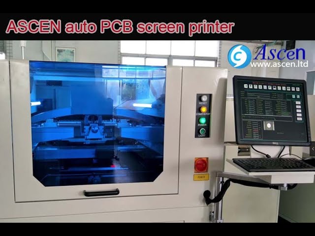
https://www.ascen.ltd/Products/Solder_paste_printer/513.html full auto PCB screen printer and SMT solder paste printing machine with Image and optical system,It is a very accurate fully automatic SMT stencil printer.automatic PCB screen printer main
https://www.ascen.ltd/Products/Solder_paste_printer/513.html full auto PCB screen printer and SMT solder paste printing machine with Image and optical system,It is a very accurate fully automatic SMT stencil printer.automatic PCB screen printer main
Events Calendar | Mon Apr 23 00:00:00 EDT 2018 - Thu Apr 26 00:00:00 EDT 2018 | Shanghai, China
SMTA China East Conference 2018
Career Center | Tustin, California USA | Engineering
REI is seeking a bi-lingual (English/Japanese) surface mount technology (SMT) Manufacturing Engineer with printed circuit board (PCB) design and manufacturing experience to join our California Operations Group. The SMT Manufacturing Engineer will de
Career Center | Tampa, Florida USA | Engineering,Management,Research and Development,Sales/Marketing,Technical Support
Spartronics is more than just a company. We have great facilities, a dedicated and talented team, tremendous capacity and capabilities, and longstanding customers who need us. Now, it’s all about driving forward with a winning strategy that bui
Career Center | Reno, Nevada USA | Engineering,Maintenance,Production,Quality Control,Research and Development,Sales/Marketing,Technical Support
Extensive technical background including tenures providing robotics technology expertise to diverse national and international clients and supporting surface mount technologies for printed circuit board (PCB) manufacturing processes. Results-oriente
SMTnet Express, June 27, 2019, Subscribers: 32,092, Companies: 10,819, Users: 24,882 Advanced Cu Electroplating Process for Any Layer Via Fill Applications with Thin Surface Copper Credits: MacDermid Inc. Copper-filled micro-vias are a key
| https://www.eptac.com/blog/3d-printing-creates-new-possibilities-for-pcb-manufacturing-methods
. Furthermore, printing PCBs in-house allows developers to test ideas that might otherwise be too costly and time consuming. By using a 3D printer, a team can design and print a new PCB prototype in-house and test it internally, allowing them to easily iterate their designs, improve their workflow and quality control, and
| https://unisoft-cim.com/pcbtest.php
drawings can either be printed or save to a file (PDF Adobe, etc.) or displayed on the screen. Create annotation overlays for Test setup notes, etc. Map Test Probe Numbers Find shorts between traces, netlists, netnames, component information, etc. The trial


