Industry Directory | Distributor
UniversityWafer is a leading silicon wafer and semiconductor substrate supplier to for academia and industry. We provide high-quality, low cost wafers in small and large quantities. Why buy wafers in volume when you don't to!
Industry Directory | Manufacturer
Full service supplier of silicon wafers and wafer processing services, including polishing, reclaim, thermal oxide and back-grinding. Supplies silicon wafers in all specifications from 2in. to 300mm in diameter.
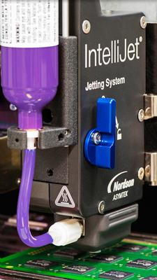
The IntelliJet® Jetting System with patented ReadiSet™ Jet Cartridge delivers cutting-edge reliability and micro dot dispensing for manufacturing advanced semiconductor and mobile electronics packages The piezo-driven IntelliJet system is the world'
Full service supplier of silicon wafers and wafer processing services, including polishing, reclaim, thermal oxide and back-grinding. Supplies silicon wafers in all specifications from 2in. to 300mm in diameter.
Electronics Forum | Tue Feb 02 09:51:38 EST 1999 | Justin Medernach
| Hello Everybody: | | I am in urgent need of some information regarding the reflow profile for a flip chip wafer. Would the reflow conditions along with the flux used affect the appearence of the solder joints. | | We are witnessing dull solder j
Electronics Forum | Tue Jul 25 16:08:52 EDT 2017 | dontfeedphils
I'm currently working on bringing a manual coating process/workcenter online and my QA team is giving me some grief. For background, we're using Humiseal 1B31 thinned with thinner 521, mixed at 1:1 by volume. Spraying through a Binks HVLP with 10 P
Used SMT Equipment | Semiconductor & Solar
· Dual Magnification, auto-focusing Optical System · DC brushless, 60,000 RPM closed-loop speed-controlled Air Bearing Spindle · Front loaded dual Cassette Compartment · Inspection Drawer - also used for single wafer load/unload · Dress Wafe
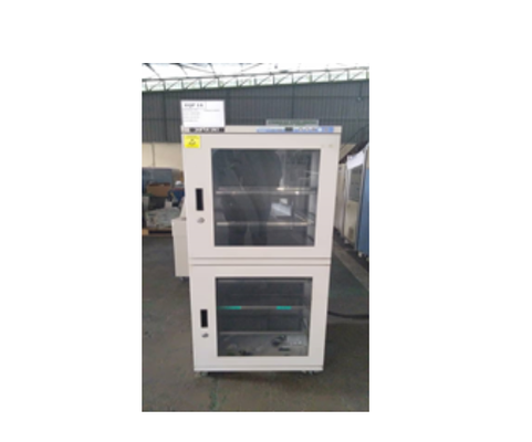
Used SMT Equipment | Drying Equipment
BRAND : SUPER DRY -02 SERIES MODEL : SD-3032-02 DESCRIPTIONS : "02 series are equipped with 1 patented dry unit to constantly main
Industry News | 2018-12-08 03:20:37.0
Top Silicon Wafer Manufacturing Companies in the World
Industry News | 2021-08-13 12:11:05.0
The Wafer-Level Packaging Symposium is scheduled for February 15-17, 2022 in San Jose, CA, USA. The theme of the event is "Advanced Packaging: The Dawn of a New Era." The development of Advanced Package Technology is undergoing a massive change because Electrical System Architects are directly driving package performance requirements.
Parts & Supplies | SMT Equipment
Specifications: Brand Name JUKI PLASTIC RAIL Part number 40046786 Model TSUBAKI TKP0450 58B R95 Ensure Test in machine confirmation Guarantee 1 month usage for machine FX-3 FX-3R Supply all JUKI motors at lower price JUKI 40034750 R3
Parts & Supplies | SMT Equipment
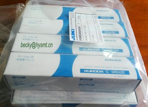
JUKI YC or Z GREASE MGREAS050GA 40031411 BARE ADJUSTMENT JIG 40031620 LOAD CELL ASM HLC-5N 40031754 I-CX PCB 40031812 LINEAR SCALE X ASM 40031860 Y BEAR CABLES ASM 40031861 XY BEAR HEAD CABLES ASM 40032048 IN STEPPING MOTOR ASM 40032049 OUT
Technical Library | 2012-02-02 19:09:53.0
A miniaturized wafer-level packaged MEMS acceleration switch with through silicon vias (TSVs) was fabricated, based on technologies suitable for harsh environment applications. The high aspect ratio TSVs were fabricated through the silicon-on-insulator (S
The Foundation for Scientific and Industrial Research - SINTEF
Technical Library | 1999-08-05 10:45:36.0
In 1998, the International 300 mm Initiative (I300I) demonstration and characterization programs will focus on 180 nm technology capability. To support these activities, I300I and equipment supplier demonstration partners must use starting silicon wafers with key parameters specified at a level appropriate level for 180 nm processing, including contamination and lithographic patterning. This document describes I300I's silicon wafer specifications, as developed with the I300I Silicon Working Group (member company technical advisors) and SEMI Standards.
Why you should attend International Wafer-Level Packaging Conference, October 23 - 25, 2018 in San Jose, California, USA.

This is the first in a series of 10-minute videos to introduce new users to the basics of machine vision technology. In this video, users will learn what machine vision is, how it is used in factory automation, and its four most common applications.
Training Courses | | | PCB Design Courses
The PCB design courses teach students the process, techniques and tools needed to design layout of printed circuit boards.
Events Calendar | Tue Feb 15 00:00:00 EST 2022 - Thu Feb 17 00:00:00 EST 2022 | San Jose, California USA
Wafer-Level Packaging Symposium
Events Calendar | Wed Feb 14 00:00:00 EST 2024 - Fri Feb 16 00:00:00 EST 2024 | San Francisco, California USA
Wafer-Level Packaging Symposium
Career Center | Charlton, Massachusetts USA | Engineering,Management,Production,Research and Development
MANUFACTURING / PROCESS ENGINEER Fused Fiber Optics company is seeking a Process Engineer to support its Optical Fabrication department. This position will be responsible for process development, optimization and troubleshooting, as well as the prep
Career Center | NORTHRIDGE, California USA | Engineering
EDUCATION BS Electronics and Communication Engineering Gujarat University MS Electrical Engineering California State University, Northridge ACADAMIC PROJECT Fabrication and Characterization of Silicon Carbide (SiC) MESFE
Career Center | Melbourne, Florida USA | Management,Production,Quality Control
Technical Skills/Abilities: � Management � Quality Assurance � Strong Troubleshooting Skills � Strategic Planning � Employee Training � Quality Assurance � Problem Resolution � Mechanical/Technical Aptitude
SMTnet Express April 25, 2013, Subscribers: 26322, Members: Companies: 13358, Users: 34615 Determination of Copper Foil Surface Roughness from Micro-section Photographs by: Scott Hinaga, Soumya De, Aleksandr Y. Gafarov, Marina Y. Koledintseva
Wafer-Level Packaged MEMS Switch With TSV Wafer-Level Packaged MEMS Switch With TSV by: Nicolas Lietaer, Thor Bakke, Anand Summanwar; SINTEF , Per Dalsjø, Jakob Gakkestad; Norwegian Defence Research Establishment (FFI), Frank Niklaus; KTH - Royal
ASYMTEK Products | Nordson Electronics Solutions | https://www.nordson.com/en/divisions/dage/wafer-inspection-and-metrology
inline and lab based X-ray inspection and metrology solutions for assessing and monitoring wafer level quality. Check shape, fill level and voiding in TSV through silicon vias
| https://productronica.com/en/trade-fair/key-topics/power-electronics/
. And Bosch plans to expand its wafer fab for SiC chips in Reutlingen by another 3,000 square meters by the end of 2023. Silicon carbide and gallium nitride


