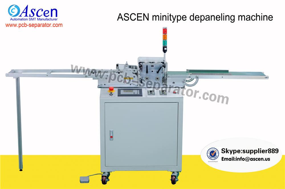
ASCEN-PCB multi cutter separator applies to automatic online separate the PCB board. At the same time, the minimum cutting length can achieve 100mm and no limits of the cutting length. High efficiency multi cutter PCB depeneling machine's minimu
Panasonic AM100 SMT Pick and Place Machine If you could not find any similar items you want, you may send some photos to us. because our catalog and website haven't included allof our products. Pick and place machine, SMT pick and place machine
Electronics Forum | Thu May 18 08:12:22 EDT 2006 | marc
smt You should have no issue using your exsisting oven for both leaded and lead free materials if the machine is capable of delivering the desired profiles. One aspect that makes a "lead free" oven is the design of the system. Ability to reach th
Electronics Forum | Wed Jun 04 18:46:10 EDT 2014 | hegemon
Well, we cannot make the cuts any deeper as then > we would incur a significant amount of "bowing" > at SMT placement/reflow. Interesting. Could be a number of factors contributing. Here's a story.... In the beginning was the board design, and in
Used SMT Equipment | Pick and Place/Feeders
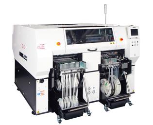
Panasonic NPM-W2 PCB mounter machine The new NPM-W2 amplifies the original NPM-W capabilities with a 10% throughput boost and 25% more accuracy. It also integrates new innovations like our incomparable Multi Recognition Camera. Combined, these feat

Used SMT Equipment | Pick and Place/Feeders
Panasonic NPM-W2 PCB mounter machine The new NPM-W2 amplifies the original NPM-W capabilities with a 10% throughput boost and 25% more accuracy. It also integrates new innovations like our incomparable Multi Recognition Camera. Combined, these feat
Industry News | 2017-10-17 19:32:15.0
MIRTEC, “The Global Leader in Inspection Technology,” is pleased to announce plans to exhibit its award-winning MV-6 OMNI 3D AOI System in Hall A2, Booth 329 at productronica 2017, scheduled to take place Nov. 14 – 17, 2017 at the Messe München in Germany. Additionally, the company will show the MS-11e 3D SPI, MV-3 OMNI Desktop 3D AOI and INTELLISYS® software.
Industry News | 2008-02-28 21:48:17.0
OXFORD, CT � February 2008 � MIRTEC a leading global supplier of AOI systems to the electronics manufacturing industry, announces that it will introduce its MV series of AOI systems in booth 1857 at the upcoming APEX exhibition & conference scheduled to take place April 1-3, 2008 in Las Vegas.
Technical Library | 2019-05-15 22:26:02.0
As the demand for higher routing density and transfer speed increases, Via-In-Pad Plated Over (VIPPO) has become more common on high-end telecommunications products. The interactions of VIPPO with other features used on a PCB such as the traditional dog-bone pad design could induce solder joints to separate during the second and thereafter reflows. The failure has been successfully reproduced, and the typical failure signature of a joint separation has been summarized.To better understand the solder separation mechanism, this study focuses on designing a test vehicle to address the following three perspectives: PCB material properties, specifically the Z-direction or out-of-plane Coefficient of Thermal Expansion (CTE); PCB thickness and back drill depth; and quantification of the driving force magnitude beyond which the separation is due to occur.
Technical Library | 2020-07-29 19:58:48.0
The majority of flexible circuits are made by patterning copper metal that is laminated to a flexible substrate, which is usually polyimide film of varying thickness. An increasingly popular method to meet the need for lower cost circuitry is the use of aluminum on Polyester (Al-PET) substrates. This material is gaining popularity and has found wide use in RFID tags, low cost LED lighting and other single-layer circuits. However, both aluminum and PET have their own constraints and require special processing to make finished circuits. Aluminum is not easy to solder components to at low temperatures and PET cannot withstand high temperatures. Soldering to these materials requires either an additional surface treatment or the use of conductive epoxy to attach components. Surface treatment of aluminum includes the likes of Electroless Nickel Immersion Gold plating (ENIG), which is extensive wet-chemistry and cost-prohibitive for mass adoption. Conductive adhesives, including Anisotropic Conductive Paste (ACP), are another alternate to soldering components. These result in component substrate interfaces that are inferior to conventional solders in terms of performance and reliability. An advanced surface treatment technology will be presented that addresses all these constraints. Once applied on Aluminum surfaces using conventional printing techniques such as screen, stencil, etc., it is cured thermally in a convection oven at low temperatures. This surface treatment is non-conductive. To attach a component, a solder bump on the component or solder printed on the treated pad is needed before placing the component. The Aluminum circuit will pass through a reflow oven, as is commonly done in PCB manufacturing. This allows for the formation of a true metal to metal bond between the solder and the aluminum on the pads. This process paves the way for large scale, low cost manufacturing of Al-PET circuits. We will also discuss details of the process used to make functional aluminum circuits, study the resultant solder-aluminum bond, shear results and SEM/ EDS analysis.
Panasonic AM100 SMT Pick and Place Machine If you could not find any similar items you want, you may send some photos to us. because our catalog and website haven't included allof our products. Pick and place machine, SMT pick and place machine
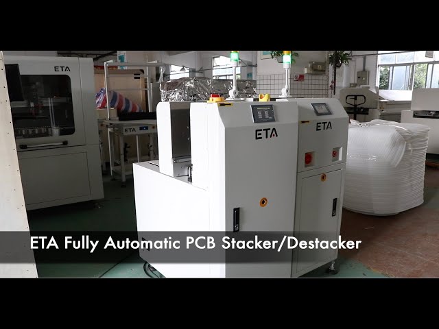
ETA SMT PCB Stacker/Destacker If you could not find any similar items you want, you may send some photos to us. because our catalog and website haven't included all of our products. PCB conveyor, PCB magazine loader, PCBA coating conveyor, pcb
Career Center | Theni, Tamilnadu India | Engineering
NPI Engineer: • Playing a role as NPI leader of the Telecom, Aerospace & Server Products to introduce and run to qualify the engineering build from customer. • Conducting Weekly NPI meeting with the CFT team to review the progress of the NPI schedu
Influence of Pd Thickness on Micro Void Formation of Solder Joints in ENEPIG Surface Finish SMTnet Express December 13, 2012, Subscribers: 26067, Members: Companies: 9068, Users: 34058 Influence of Pd Thickness on Micro Void Formation of Solder
| http://etasmt.com/cc?ID=te_news_industry,23961&url=_print
Case study: How to Create a Reflow Profile for a 16-layer, 2mm Thickness PCB with a High Density SMT Connector?-SMT Technical-Reflow oven,SMT Reflow Soldering Oven-cmsadmin Reflow oven,SMT Reflow Soldering Oven 当前位置: Home >> News
| https://www.smtfactory.com/Live-Update-I-C-T-at-The-ExpoElectronica-Exhibition-in-Moscow-id43001537.html
【Live Update】I.C.T at The ExpoElectronica Exhibition in Moscow - I.C.T SMT Machine English Bahasa indonesia Сербия Česky Dansk Deutsch Español


