New Equipment | Cleaning Agents
LONOX® L5611 is a solvent-based cleaner for misprinted boards and stencils. It is effective on a wide variety of flux, solder paste and uncured adhesives. Easy to use, L5611 is intended to be diluted with water and effective at ambient temperature t
Electronics Forum | Sun Nov 08 15:27:25 EST 2015 | davef
Thinner: Flux thinner, NOT paint thinner We kept a spare stone in thinner in inventory. We cut PVC pipe to size, cap in one end, screw thread on the other, stone inside, filled with flux thinner and covered with a screw cap. I don't remember who we
Electronics Forum | Wed Sep 27 13:45:35 EDT 2000 | Bill Schreiber
Dear Dreamsniper, A big hidden cost in any cleaning system is the cost of diminished production and rework. I assume you are cleaning the adhesive stencils manually since there is no equipment cost in your formula. Manual cleaning of adhesive sten
Industry News | 2018-12-08 03:38:44.0
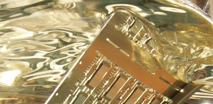
Lead-Free (Pb-Free) Solder and Composition
Industry News | 2018-12-08 03:29:29.0
SMT Dictionary – Surface Mount Technology Acronym and Abbreviation
Technical Library | 2020-08-27 01:22:45.0
Initially adopted internal specifications for acceptance of printed circuit boards (PCBs) used for wire bonding was that there were no nodules or scratches allowed on the wirebond pads when inspected under 20X magnification. The nodules and scratches were not defined by measurable dimensions and were considered to be unacceptable if there was any sign of a visual blemish on wire-bondable features. Analysis of the yield at a PCB manufacturer monitored monthly for over two years indicated that the target yield could not be achieved, and the main reasons for yield loss were due to nodules and scratches on the wirebonding pads. The PCB manufacturer attempted to eliminate nodules and scratches. First, a light-scrubbing step was added after electroless copper plating to remove any co-deposited fine particles that acted as a seed for nodules at the time of copper plating. Then, the electrolytic copper plating tank was emptied, fully cleaned, and filtered to eliminate the possibility of co-deposited particles in the electroplating process. Both actions greatly reduced the density of the nodules but did not fully eliminate them. Even though there was only one nodule on any wire-bonding pad, the board was still considered a reject. To reduce scratches on wirebonding pads, the PCB manufacturer utilized foam trays after routing the boards so that they did not make direct contact with other boards. This action significantly reduced the scratches on wire-bonding pads, even though some isolated scratches still appeared from time to time, which caused the boards to be rejected. Even with these significant improvements, the target yield remained unachievable. Another approach was then taken to consider if wire bonding could be successfully performed over nodules and scratches and if there was a dimensional threshold where wire bonding could be successful. A gold ball bonding process called either stand-off-stitch bonding (SSB) or ball-stitch-on-ball bonding (BSOB) was used to determine the effects of nodules and scratches on wire bonds. The dimension of nodules, including height, and the size of scratches, including width, were measured before wire bonding. Wire bonding was then performed directly on various sizes of nodules and scratches on the bonding pad, and the evaluation of wire bonds was conducted using wire pull tests before and after reliability testing. Based on the results of the wire-bonding evaluation, the internal specification for nodules and scratches for wirebondable PCBs was modified to allow nodules and scratches with a certain height and a width limitation compared to initially adopted internal specifications of no nodules and no scratches. Such an approach resulted in improved yield at the PCB manufacturer.

ALPHA® Preforms with solder paste adds solder volume.
Events Calendar | Tue Apr 13 00:00:00 EDT 2021 - Tue Apr 13 00:00:00 EDT 2021 | ,
Boston Chapter Webinar: Cleaning Chemistry For PWB and Rework - Part 2, session 1
Events Calendar | Tue Apr 13 00:00:00 EDT 2021 - Tue Apr 13 00:00:00 EDT 2021 | ,
Boston Chapter Webinar: Cleaning Chemistry For PWB and Rework - Part 2, session 2
ASYMTEK Products | Nordson Electronics Solutions | https://www.nordson.com/en/divisions/adhesive-dispensing-systems/industries/construction-and-architectural/cable-manufacturing?con=t&page=12
. Nordson VersaPUR Adhesive Melters Simplify Use of Reactive Polyurethane Adhesives - News Release Adhesive Dispensing Systems Easy-to-clean Nordson VersaPUR tank melters for PUR adhesives Freedom®
Blackfox Training Institute, LLC | https://www.blackfox.com/blog/guide-to-a-successful-lead-free-soldering/
. Lead-free soldering produces a clean and excellent finish and has less risk of corrosion. For this reason, lead-free soldering is used in many of the latest consumer electronics that we use today


