New Equipment | Education/Training
This specification covers qualification and performance of rigid PCBs including with or without plated-through holes, single-sided, double-sided, multilayer with or without blind/buried vias and metal core boards. It addresses final finish and surfac
IPC 6012 Qualification and Performance Specification for Rigid Printed Boards This specification covers qualification and performance of rigid PCBs including with or without plated-through holes, single-sided, double-sided, multilayer with or withou
Electronics Forum | Wed Jul 07 09:47:41 EDT 1999 | Peter Brant
| | Q #1) Is it more reliable to have the mask tent over the vias or risk getting vias half filled with solder? These are vias with an .020" hole and .040" or .050" pad. WIth regards to this question, and scott's follow up, I have used the "epoxy me
Electronics Forum | Tue Jul 06 19:38:01 EDT 1999 | John
Q #1) Is it more reliable to have the mask tent over the vias or risk getting vias half filled with solder? These are vias with an .020" hole and .040" or .050" pad. Q #2) When speaking of annular rings, I have always thought of them as minimums. Su
Industry News | 2003-03-11 08:45:00.0
CAMtastic DXP is the latest version of Altium's complete CAM verification and editing system that bridges the gap between PCB design and manufacturing and facilitates communication between board designers, fabrication engineers, and their clients.
Industry News | 2012-09-10 12:48:23.0
To help companies gain the most out of HDI technology, Raytheon is sponsoring the “IPC HDI Conference: Advancements in Materials, Processes and Applications,” October 24–25 in Los Angeles, Calif.
Technical Library | 2019-07-17 17:56:34.0
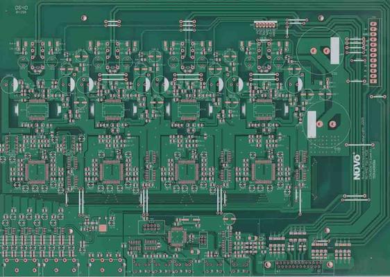
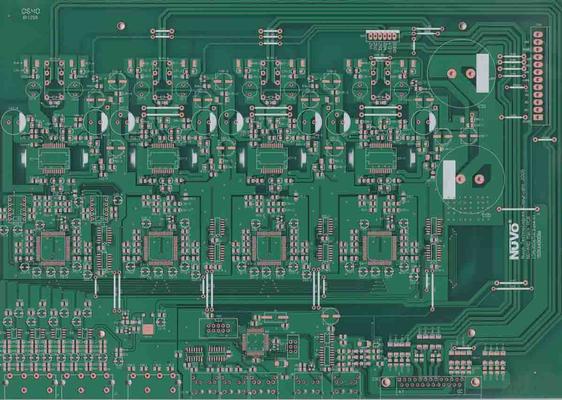
The increased demand for electronic devices in recent years has led to an extensive research in the field to meet the requirements of the industry. Electrolytic copper has been an important technology in the fabrication of PCBs and semiconductors. Aqueous sulfuric acid baths are explored for filling or building up with copper structures like blind micro vias (BMV), trenches, through holes (TH), and pillar bumps. As circuit miniaturization continues, developing a process that simultaneously fills vias and plates TH with various sizes and aspect ratios, while minimizing the surface copper thickness is critical. Filling BMV and plating TH at the same time, presents great difficulties for the PCB manufactures. The conventional copper plating processes that provide good via fill and leveling of the deposit tend to worsen the throwing power (TP) of the electroplating bath. TP is defined as the ratio of the deposit copper thickness in the center of the through hole to its thickness at the surface. In this paper an optimization of recently developed innovative, one step acid copper plating technology for filling vias with a minimal surface thickness and plating through holes is presented.
Technical Library | 2021-06-21 19:34:02.0
In this era of electronics miniaturization, high yield and low-cost integrated circuit (IC) substrates play a crucial role by providing a reliable method of high density interconnection of chip to board. In order to maximize substrate real-estate, the distance between Cu traces also known as line and space (L/S) should be minimized. Typical PCB technology consists of L/S larger than 40 µ whereas more advanced wafer level technology currently sits at or around 2 µm L/S. In the past decade, the chip size has decreased significantly along with the L/S on the substrate. The decreasing chip scales and smaller L/S distances has created unique challenges for both printed circuit board (PCB) industry and the semiconductor industry. Fan-out panel-level packaging (FOPLP) is a new manufacturing technology that seeks to bring the PCB world and IC/semiconductor world even closer. While FOPLP is still an emerging technology, the amount of high-volume production in this market space provide a financial incentive to develop innovative solutions in order to enable its ramp up. The most important performance aspect of the fine line plating in this market space is plating uniformity or planarity. Plating uniformity, trace/via top planarity, which measures how flat the top of the traces and vias are a few major features. This is especially important in multilayer processing, as nonuniformity on a lower layer can be transferred to successive layers, disrupting the device design with catastrophic consequences such as short circuits. Additionally, a non-planar surface could also result in signal transmission loss by distortion of the connecting points, like vias and traces. Therefore, plating solutions that provide a uniform, planar profile without any special post treatment are quite desirable.

This video describes the IPC A-600 training and certification program. The IPC A-600 specification is a set of acceptability specifications for printed circuit boards. These standards determine the acceptance and reject criteria for printed wiring bo
This video describes the IPC A-600 training and certification program. The IPC A-600 specification is a set of acceptability specifications for printed circuit boards. These standards determine the acceptance and reject criteria for printed wiring bo
Training Courses | ON DEMAND | | IPC-600 Trainer (CIT)
The Certified IPC-600 Trainer (CIT) courses recognize individuals as qualified trainers in the area of quality assurance of bare printed circuit boards and prepare them to deliver Certified IPC-600 (CIS) training.
SMTnet Express, July 16, 2020, Subscribers: 28,512, Companies: 11,045, Users: 25,964 Via In Pad - Conductive Fill or Non-Conductive Fill? Credits: Advanced Circuits In the early 2000s the first fine-pitch ball grid array devices became popular
SMTnet Express, June 27, 2019, Subscribers: 32,092, Companies: 10,819, Users: 24,882 Advanced Cu Electroplating Process for Any Layer Via Fill Applications with Thin Surface Copper Credits: MacDermid Inc. Copper-filled micro-vias are a key
PCB Libraries, Inc. | https://www.pcblibraries.com/forum/RSS_pcb-via-terms-and-applications_topic1596.xml
PCB Libraries Forum : PCB Via Terms and Applications PCB Libraries Forum : PCB Via Terms and Applications This is an XML content feed of
Surface Mount Technology Association (SMTA) | https://www.smta.org/education/presentations/presentations.cfm
form a reliable joint with the assembly process automated if volumes require. Through hole paste reflow can benefit using solder bricks to increase joint volume and decrease flux residues. Some placement machine suppliers offer produced cut and form


