New Equipment | Assembly Services
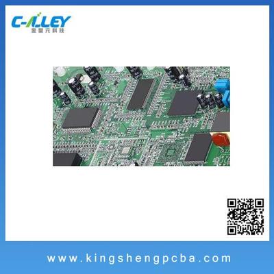
Our Service PCB Assembly and PCB&PCBA design are our main business.We are able to undertake a high quality Printed Circuit Board Assembly on competitive prices and flexible conditions.We are a complete “One- Stop” resource for printed circuit board
Electronics Forum | Fri Aug 16 10:00:03 EDT 2002 | davef
You have a very bad situation. It�s tough for the gas, flux material, er whatever to escape when the BGA is sitting on top of it and the blind via is blocking it from the other side. Obviously the vias should have been: * Placed on the edge of the
Electronics Forum | Tue Sep 17 15:03:31 EDT 2002 | davef
Contact: * PCD Magazine [ http://www.pcdmag.com/mag/reprints.html ] and ask them to send you a reprint. * Jim Blankenhorn [ http://www.smtplus.com ] and ask him to send you a reprint. Or try: * �Assembly And Interconnect Reliability Of BGA Assembled
Industry News | 2018-12-08 03:29:29.0
SMT Dictionary – Surface Mount Technology Acronym and Abbreviation
SMTnet Express, October 10, 2019, Subscribers: 32,263, Companies: 10,893, Users: 25,93 Fill the Void IV: Elimination of Inter-Via Voiding Credits: FCT ASSEMBLY, INC. Voids are a plague to our electronics and must be eliminated! Over the last few
SMTnet Express March 7, 2013, Subscribers: 26214, Members: Companies: 13311, Users: 34412 PTH Core-to-Core Interconnect Using Sintered Conductive Pastes The market for high-layer-count printed circuit boards (PCB) containing blind and buried vias
Heller Industries Inc. | https://hellerindustries.com/wp-content/uploads/2022/04/last-will-of-bga-void-1.pdf
: A total of 21 of 40 test vehicles had a void greater than 45% of solder ball diameter or 20% of ball area Solder crack path typically found at solder joint / BGA package interface Via in Pad (VIP
Imagineering, Inc. | https://www.pcbnet.com/capabilities/assembly/technology-roadmap/
. Layer Count 50 Max. Working Panel Size 21" x 31" Max. Board Thickness .300" Min. Board Thickness 0.16"(6L) Min. Line/Space • I/L - 2 / 1.5mil (HDI) • O/L - 2 / 1.5 mil (HDI) Warpage .001" / sq. in. BGA Pitch 0.20mm Layer to Layer Registration 3 mil


.gif)
winsouce.jpg)