
http://www.ddmnovastar.com/stencil-printers - DDM Novastar Stencil Printers are designed for short to medium run PCB assembly. Ranging from manual to semi-automatic, these durable, easy-to-use systems provide repeatable, reliable results. Greatly r
http://www.ddmnovastar.com/stencil-printers - DDM Novastar Stencil Printers are designed for short to medium run PCB assembly. Ranging from manual to semi-automatic, these durable, easy-to-use systems provide repeatable, reliable results. Greatly r
http://www.ddmnovastar.com/stencil-printers - DDM Novastar Stencil Printers are designed for short to medium run PCB assembly. Ranging from manual to semi-automatic, these durable, easy-to-use systems provide repeatable, reliable results. Greatly r
Industry News | 2018-10-18 08:39:14.0
Stencil Technology for SMT production
Technical Library | 2015-08-25 13:51:27.0
The stencil printing process is one of the most critical processes in the electronic production. Due to the requirement: "faster and smaller" it is necessary to place components with different paste volume close together without regard to solder paste printing. In our days it is no longer possible to control the solder paste volume only by adjustment of the aperture dimensions. The requirements of solder paste volumes for specific components are realized by different thicknesses of metal sheets in one stencil with so called step stencils. The step-down stencil is required when it is desirable to print fine-pitch devices using a thinner stencil foil, but print other devices using a thicker stencil foil. The paper presents the innovative technology of step-up and step-down stencils in a laser cutting and laser welding process. The step-up/step-down stencil is a special development for the adjustment of solder paste quantity, fulfilling the needs of placement and soldering. This includes the laser cutting and laser welding process as well as the resulting stencil characteristics and the potential of the printing process.
Technical Library | 2023-07-25 16:25:56.0
This paper address two significant applications of stencils in advance packaging field: 1. Ultra-Thin stencils for miniature component (0201m) assembly; 2. Deep Cavity stencils for embedded (open cavity) packaging. As the world of electronics continues to evolve with focus on smaller, lighter, faster, and feature-enhanced high- performing electronic products, so are the requirement for complex stencils to assemble such components. These stencil thicknesses start from less than 25um with apertures as small as 60um (or less). Step stencils are used when varying stencil thicknesses are required to print into cavities or on elevated surfaces or to provide relief for certain features on a board. In the early days of SMT assembly, step stencils were used to reduce the stencil thickness for 25 mil pitch leaded device apertures. Thick metal stencils that have both relief-etch pockets and reservoir step pockets are very useful for paste reservoir printing. Electroform Step-Up Stencils for ceramic BGA's and RF Shields are a good solution to achieve additional solder paste height on the pads of these components as well as providing exceptional paste transfer for smaller components like uBGAs and 0201s. As the components are getting smaller, for example 0201m, or as the available real estate for component placement on a board is getting smaller – finer is the aperture size and the pitch on the stencils. Aggressive distances from step wall to aperture are also required. Ultra-thin stencils with thicknesses in the order of 15um-40um with steps of 15um are used to obtain desired print volumes. Stencils with thickness to this order can be potential tools even to print for RDLs in the package.
Technical Library | 2023-07-25 16:42:54.0
Printing solder paste for very small components like .3mm pitch CSP's and 01005 Chip Components is a challenge for the printing process when other larger components like RF shields, SMT Connectors, and large chip or resistor components are also present on the PCB. The smaller components require a stencil thickness typically of 3 mils (75u) to keep the Area Ratio greater than .55 for good paste transfer efficiency. The larger components require either more solder paste height or volume, thus a stencil thickness in the range of 4 to 5 mils (100 to 125u). This paper will explore two stencil solutions to solve this dilemma. The first is a "Two Print Stencil" option where the small component apertures are printed with a thin stencil and the larger components with a thicker stencil with relief pockets for the first print. Successful prints with Keep-Outs as small as 15 mils (400u) will be demonstrated. The second solution is a stencil technology that will provide good paste transfer efficiency for Area Ratio's below .5. In this case a thicker stencil can be utilized to print all components. Paste transfer results for several different stencil types including Laser-Cut Fine Grain stainless steel, Laser-Cut stainless steel with and w/o PTFE Teflon coating, AMTX E-FAB with and w/o PTFE coating for Area Ratios ranging from .4 up to .69.
Industry News | 2017-07-09 20:40:11.0
SHENMAO Technology, Inc. introduces New Generation Ultra Tacky Flux SMF-WC52 applied in the Flip Chip dipping process. Its high tacky property keeps Chip in place during reflow for excellent soldering performance, while creating outstanding solder joint strength.
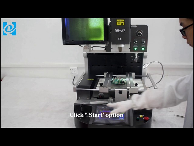
Dinghua Technology-- the leading manufacturer of BGA rework station, Automatic screw locking machine, Automatic soldering station and non-standard equipment. For more details, please just contact John, WhatsApp/Wechat:+86 1576811 4827 , Skype: si
Technical Library | 2018-03-07 22:41:05.0
This study investigates the scooping effect during solder paste printing as a function of aperture width, aperture length and squeegee pressure. The percent of the theoretical volume deposited depends on the PWB topography. A typical bimodal percent volume distribution is attributed to poor release apertures and large apertures, where scooping takes place, yielding percent volumes 100%. This printing experiment is done with a concomitant validation of the printing process using standard 3D Solder Paste Inspection (SPI) equipment.


