Technical Library | 2021-05-26 00:53:26.0
This paper describes a copper electroplating enabling technology for filling microvias. Driven by the need for faster, smaller and higher performance communication and electronic devices, build-up technology incorporating microvias has emerged as a viable multilayer printed circuit manufacturing technology. Increased wiring density, reduced line widths, smaller through-holes and microvias are all attributes of these High Density Interconnect (HDI) packages. Filling the microvias with conductive material allows the use of stacked vias and via in pad designs thereby facilitating additional packaging density. Other potential design attributes include thermal management enhancement and benefits for high frequency circuitry. Electrodeposited copper can be utilized for filling microvias and provides potential advantages over alternative via plugging techniques. The features, development, scale up and results of direct current (DC) and periodic pulse reverse (PPR) acid copper via filling processes, including chemistry and equipment, are described.

Innovative Materials, Superior Performance. Our printed circuit board and semiconductor packaging materials provide superior thermal and mechanical performance, a fact we’ve prided ourselves on for over 45 years. All our materials are RoHS complian
Technical Library | 2020-07-15 18:29:34.0
In the early 2000s the first fine-pitch ball grid array devices became popular with designers looking to pack as much horsepower into as small a space as possible. "Smaller is better" became the rule and with that the mechanical drilling world became severely impacted by available drill bit sizes, aspect ratios, and plating methodologies. First of all, the diameter of the drill needed to be in the 0.006" or smaller range due to the reduction of pad size and spacing pitch. Secondly, the aspect ratio (depth to diameter) became limited by drill flute length, positional accuracy, rigidity of the tools (to prevent breakage), and the throwing power of acid copper plating systems. And lastly, the plating needed to close up the hole as much as possible, which led to problems with voiding, incomplete fill, and gas/solution entrapment.
IPC 6012 Qualification and Performance Specification for Rigid Printed Boards This specification covers qualification and performance of rigid PCBs including with or without plated-through holes, single-sided, double-sided, multilayer with or withou
Industry Directory | Manufacturer
Manufacturer of sintering, electrically conductive materials. Applications include semiconductor die attach, component attach, via fill, z-axis interconnection, conductive lines and traces and plated-through hole fill.

SIPAD Systems Incorporated (SSi) is the Exclusive Supplier of SIPAD solid solder deposit in North America and the only SIPAD Solid Solder Deposit (SSD) coating service bureau in the world. SIPAD Systems Inc. supplies SIPAD solid solder coating servi
Industry Directory | Manufacturer
We specialize in Flex PCBs, Ridgid Flex, Long Flex PCBs and RF (radio frequency) Boards. Our engineering team has seen it all.
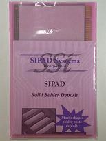
SIPAD Solid Solder Deposit (ssd) is a Siemens patented process that pre loads the pc board surface mount pads with solder in a solid form. Boards are printed, reflowed without components producing a predictable repeatable meniscus. SIPAD boards a
Parts & Supplies | Circuit Board Assembly Products
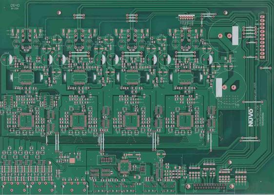
1). 100mm x 98mm/1up, FR-4, 2). 1mm +/-0.1mm,6 Layers 3). 1oz copper finished 3). Green solder mask/white legend 4). Min. hole 0.15mm, 4/4 mil track/gap 5). Blind via layer 1-2, via-in-pad. 6). Immersion gold surface finish
Technical Library | 2016-03-03 17:25:26.0
This paper discusses a nano copper based paste for use in via filling. The company manufactures nano copper and disperses the coated nano copper into a paste in combination with micron copper. The resultant paste is injected or fills a via. The via is subsequently sintered by means of photonic sintering, or by heat in a reducing environment. The process will be accomplished in under an hour and results in filled solid copper vias.


