
New Equipment | Fabrication Services
Based on the special application of PCB, Aluminum base material and Copper base material are used to replace the traditional FR-4 material. Eastech has very mature production and manufacturing experience for PCB based on metal materials. We always br
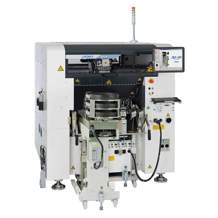
JUKI JM-20 Hybrid Pick and Place Machine Max PCB:410×560mm Component Size:0603~50mm Place Speed:15,500 CPH Product description: JUKI JM-20 Hybrid Pick and Place Machine, Max PCB:410×560mm, Component Size:0603~50mm, Place Speed:15,5

JUKI JM-20 Hybrid Pick and Place Machine Max PCB:410×560mm Component Size:0603~50mm Place Speed:15,500 CPH Product description: JUKI JM-20 Hybrid Pick and Place Machine, Max PCB:410×560mm, Component Size:0603~50mm, Place Speed:15
Technical Library | 2020-08-27 01:22:45.0
Initially adopted internal specifications for acceptance of printed circuit boards (PCBs) used for wire bonding was that there were no nodules or scratches allowed on the wirebond pads when inspected under 20X magnification. The nodules and scratches were not defined by measurable dimensions and were considered to be unacceptable if there was any sign of a visual blemish on wire-bondable features. Analysis of the yield at a PCB manufacturer monitored monthly for over two years indicated that the target yield could not be achieved, and the main reasons for yield loss were due to nodules and scratches on the wirebonding pads. The PCB manufacturer attempted to eliminate nodules and scratches. First, a light-scrubbing step was added after electroless copper plating to remove any co-deposited fine particles that acted as a seed for nodules at the time of copper plating. Then, the electrolytic copper plating tank was emptied, fully cleaned, and filtered to eliminate the possibility of co-deposited particles in the electroplating process. Both actions greatly reduced the density of the nodules but did not fully eliminate them. Even though there was only one nodule on any wire-bonding pad, the board was still considered a reject. To reduce scratches on wirebonding pads, the PCB manufacturer utilized foam trays after routing the boards so that they did not make direct contact with other boards. This action significantly reduced the scratches on wire-bonding pads, even though some isolated scratches still appeared from time to time, which caused the boards to be rejected. Even with these significant improvements, the target yield remained unachievable. Another approach was then taken to consider if wire bonding could be successfully performed over nodules and scratches and if there was a dimensional threshold where wire bonding could be successful. A gold ball bonding process called either stand-off-stitch bonding (SSB) or ball-stitch-on-ball bonding (BSOB) was used to determine the effects of nodules and scratches on wire bonds. The dimension of nodules, including height, and the size of scratches, including width, were measured before wire bonding. Wire bonding was then performed directly on various sizes of nodules and scratches on the bonding pad, and the evaluation of wire bonds was conducted using wire pull tests before and after reliability testing. Based on the results of the wire-bonding evaluation, the internal specification for nodules and scratches for wirebondable PCBs was modified to allow nodules and scratches with a certain height and a width limitation compared to initially adopted internal specifications of no nodules and no scratches. Such an approach resulted in improved yield at the PCB manufacturer.
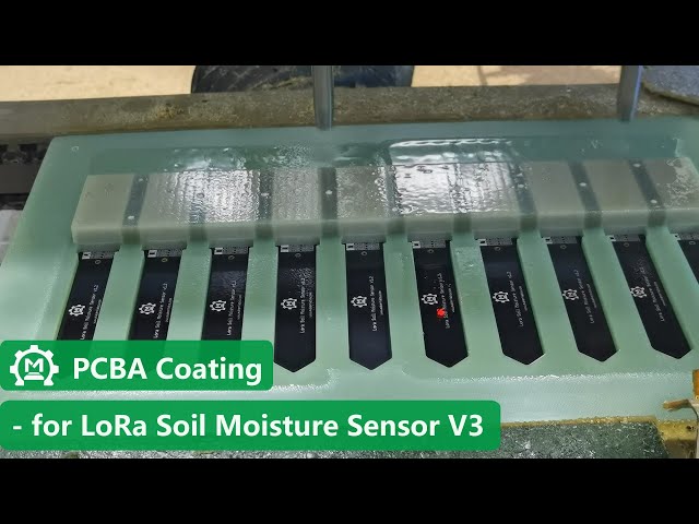
Great improvements on Makerfabs Lora Soil Moisture Sensor V3!!! 1. TLC555 removed, while the Atmega328P(D9/Timer1) generates the 2 MHz pulse (only during measurement phase, switching off afterward), for capacitive moisture measurement. 2. Unique ID b
Industry News | 2018-10-18 11:08:03.0
Different Techniques for Plating

JUKI JM-20 Hybrid Placement Machine Component Size:0603~50mm Place Max PCB:410×560mm JUKI JM-20 Hybrid Placement Machine Speed:15,500 CPH Product description: JUKI JM-20 Hybrid Placement Machine,Max PCB:410×560mm, Component Size:06

JUKI JM-20 Hybrid Placement Machine Max PCB:410×560mm Component Size:0603~50mm Place Speed:15,500 CPH Laser recognition ±0.05mm(3σ) Product description: JUKI JM-20 Multi Task Platform Hybrid Placement Machine, Max PCB:410×560mm, Component Size
Industry News | 2019-04-15 16:47:35.0
New model of LCR-Reader-MP on the horizon; updated model offers record high basic accuracy and unparalleled amount of test functions
Industry News | 2017-07-19 21:09:38.0
STI Electronics is pleased to announce the acquisition of a new Fischerscope X-ray XDAL 237 energy dispersive X-ray fluorescence (EDXRF) system.

Products, services, training & consulting for the assembly, rework & repair of electronic assemblies. BGA process experts. Manufacturers Rep, Distributor & Service Provider for Seamark/Zhuomao and Shuttle Star BGA Rework Stations.
Training Provider / Manufacturer's Representative / Equipment Dealer / Broker / Auctions / Consultant / Service Provider
1750 Mitchell Ave.
Oroville, CA USA
Phone: (888) 406-2830

.gif)


