Technical Library | 2023-07-25 16:50:02.0
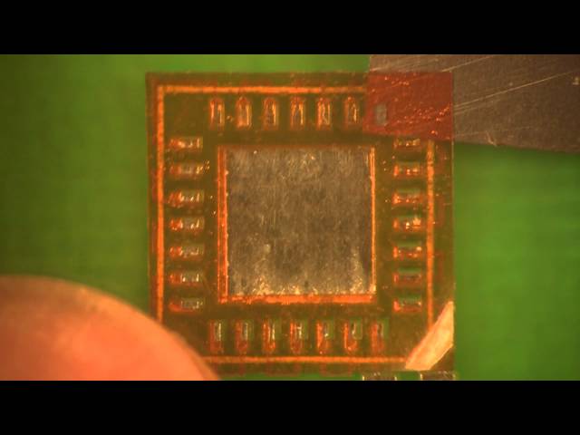
Some of the new handheld communication devices offer real challenges to the paste printing process. Normally, there are very small devices like 01005 chip components as well as 0.3 mm pitch uBGA along with other devices that require higher deposits of solder paste. Surface mount connectors or RF shields with coplanarity issues fall into this category. Aperture sizes for the small devices require a stencil thickness in the 50 to 75 um (2-3 mils) range for effective paste transfer whereas the RF shield and SMT connector would like at least 150 um (6 mils) paste height. Spacing is too small to use normal step stencils. This paper will explore a different type of step stencil for this application; a "Two-Print Stencil Process" step stencil. Here is a brief description of a "Two-Print Stencil Process". A 50 to 75 um (2-3 mils) stencil is used to print solder paste for the 01005, 0.3 mm pitch uBGA and other fine pitch components. While this paste is still wet a second in-line stencil printer is used to print all other components using a second thicker stencil. This second stencil has relief pockets on the contact side of the stencil any paste was printed with the first stencil. Design guidelines for minimum keep-out distances between the relief step, the fine pitch apertures, and the RF Shields apertures as well relief pocket height clearance of the paste printed by the first print stencil will be provided.
Technical Library | 2023-08-04 15:27:30.0
A designed experiment evaluated the influence of several variables on appearance and strength of Pb-free solder joints. Components, with leads finished with nickel-palladium-gold (NiPdAu), were used from Texas Instruments (TI) and two other integrated circuit suppliers. Pb-free solder paste used was tin-silver-copper (SnAgCu) alloy. Variables were printed wiring board (PWB) pad size/stencil aperture (the pad finish was consistent; electrolysis Ni/immersion Au), reflow atmosphere, reflow temperature, Pd thickness in the NiPdAu finish, and thermal aging. Height of solder wetting to component lead sides was measured for both ceramic plate and PWB soldering. A third response was solder joint strength; a "lead pull" test determined the maximum force needed to pull the component lead from the PWB. This paper presents a statistical analysis of the designed experiment. Reflow atmosphere and pad size/stencil aperture have the greatest contribution to the height of lead side wetting. Reflow temperature, palladium thickness, and preconditioning had very little impact on side-wetting height. For lead pull, variance in the data was relatively small and the factors tested had little impact.
Technical Library | 2024-04-08 15:46:36.0
A designed experiment evaluated the influence of several variables on appearance and strength of Pb-free solder joints. Components, with leads finished with nickel-palladium-gold (NiPdAu), were used from Texas Instruments (TI) and two other integrated circuit suppliers. Pb-free solder paste used was tin-silver-copper (SnAgCu) alloy. Variables were printed wiring board (PWB) pad size/stencil aperture (the pad finish was consistent; electrolysis Ni/immersion Au), reflow atmosphere, reflow temperature, Pd thickness in the NiPdAu finish, and thermal aging. Height of solder wetting to component lead sides was measured for both ceramic plate and PWB soldering. A third response was solder joint strength; a "lead pull" test determined the maximum force needed to pull the component lead from the PWB. This paper presents a statistical analysis of the designed experiment. Reflow atmosphere and pad size/stencil aperture have the greatest contribution to the height of lead side wetting. Reflow temperature, palladium thickness, and preconditioning had very little impact on side-wetting height. For lead pull, variance in the data was relatively small and the factors tested had little impact.
New Equipment | Solder Paste Stencils
Step-up / Step-down Stencil. The patented step stencil from LaserJob, called PatchWork® - stencil, was developed to print in one printing step different paste deposit heights. Due to the multiplicity of different component leads on one printed circu
New Equipment | Solder Paste Stencils
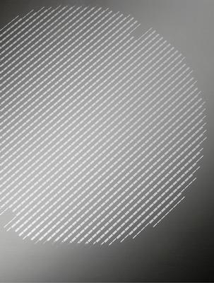
Laser cut stainless steel stencil for solder paste printing on wafer. Wafer bumping stencils are characterized by a high number of apertures which lie close together in the size of 90µm x 110µm. A package density of up to 250000 openings is not unus
.JPG)
Used SMT Equipment | SPI / Solder Paste Inspection
The LSM300 follows the successful Laser section Microscopes LSM and LSM2. This new non-contact laser based system is an off-Line solder paste inspection system.LSM300 provides automatic height measurements, eliminating the inconsistencies of manual m
Technical Library | 2023-07-25 16:25:56.0
This paper address two significant applications of stencils in advance packaging field: 1. Ultra-Thin stencils for miniature component (0201m) assembly; 2. Deep Cavity stencils for embedded (open cavity) packaging. As the world of electronics continues to evolve with focus on smaller, lighter, faster, and feature-enhanced high- performing electronic products, so are the requirement for complex stencils to assemble such components. These stencil thicknesses start from less than 25um with apertures as small as 60um (or less). Step stencils are used when varying stencil thicknesses are required to print into cavities or on elevated surfaces or to provide relief for certain features on a board. In the early days of SMT assembly, step stencils were used to reduce the stencil thickness for 25 mil pitch leaded device apertures. Thick metal stencils that have both relief-etch pockets and reservoir step pockets are very useful for paste reservoir printing. Electroform Step-Up Stencils for ceramic BGA's and RF Shields are a good solution to achieve additional solder paste height on the pads of these components as well as providing exceptional paste transfer for smaller components like uBGAs and 0201s. As the components are getting smaller, for example 0201m, or as the available real estate for component placement on a board is getting smaller – finer is the aperture size and the pitch on the stencils. Aggressive distances from step wall to aperture are also required. Ultra-thin stencils with thicknesses in the order of 15um-40um with steps of 15um are used to obtain desired print volumes. Stencils with thickness to this order can be potential tools even to print for RDLs in the package.
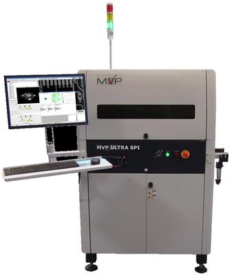
MVP’s enhanced Ultra SPI Solder Paste Inspection systems deploy our patented 3D technologies along with MVPs trusted AOI capabilities. Utilizing MVP’s patented technology, 3D Solder Paste Inspection (SPI) can be performed on paste for apertures as sm
Technical Library | 2023-05-02 19:06:43.0
As 0402 has become a common package for printed circuit board (PCB) assembly, research and development on mounting 0201 components is emerging as an important topic in the field of surface mount technology for PWB miniaturization. In this study, a test vehicle for 0201 packages was designed to investigate board design and assembly issues. Design of Experiment (DOE) was utilized, using the test vehicle, to explore the influence of key parameters in pad design, printing, pick-andplace, and reflow on the assembly process. These key parameters include printing parameters, mounting height or placement pressure, reflow ramping rate, soak time and peak temperature. The pad designs consist of rectangular pad shape, round pad shape and home-based pad shape. For each pad design, several different aperture openings on the stencil were included. The performance parameters from this experiment include solder paste height, solder paste volume and the number of post-reflow defects. By analyzing the DOE results, optimized pad designs and assembly process parameters were determined.


