Industry News | 2016-11-30 14:47:45.0
ACI Technologies invites you to download a free copy of its very popular e-booklet, “Failure Analysis Techniques for Electronics” from its Website store, which is located at http://store.aciusa.org/Failure-Analysis-Techniques-for-Electronics-Digital-Download-P181.aspx
Gold embrittlement of solder joints has been a concern for many decades. SEM Lab, Inc. supports evaluation for this condition. Gold embrittlement can be avoided by careful solder joint design and knowledge of the causes of this condition. https://s
Technical Library | 2014-08-07 15:13:44.0
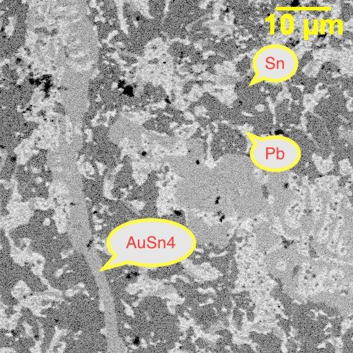
Gold embrittlement in SnPb solder is a well-known failure mechanism in electronic assembly. To avoid this issue, prior studies have indicated a maximum gold content of three weight percent. This study attempts to provide similar guidance for Pb-free (SAC305) solder. Standard surface mount devices were assembled with SnPb and SAC305 solder onto printed boards with various thicknesses of gold plating. The gold plating included electroless nickel immersion gold (ENIG) and electrolytic gold of 15, 25, 35, and 50 microinches over nickel. These gold thicknesses resulted in weight percentages between 0.4 to 7.0 weight percent.
Industry News | 2021-04-13 17:37:07.0
Gold plating dissolves rapidly during soldering and can result in gold embrittlement. This tech paper examines how to re-condition electronic components prior to soldering.
Industry News | 2021-07-26 17:33:25.0
High thermal mass and fine-pitch components place increased demand on the selective soldering process. This tech paper outlines techniques that minizine these demands.
Technical Library | 2022-08-08 15:06:06.0
Selective soldering has evolved to become a standard production process within the electronics assembly industry, and now accommodates a wide variety of through-hole component formats in numerous applications. Most through-hole components can be easily soldered with the selective soldering process without difficulty however some types of challenging components require additional attention to ensure that optimum quality is maintained. Several high thermal mass components can place demands on the selective soldering process, while the use of specialized solder fixtures, or solder pallets, often places additional thermal demand on the preheating process. Fine-pitch through-hole components and connectors place a different set of demands on the selective soldering process and typically require special attention to lead projection and traverse speed to minimize bridging between adjacent pins. Dual in-line memory module (DIMM) connectors, compact peripheral component interface (cPCI) connectors, coax connectors and other high thermal mass components as well as fine-pitch microconnectors, can present challenges when soldered into backplanes or multilayer printed circuit board assemblies. Adding to this challenge, compact peripheral component interface connectors can present additional solderability issues because of their beryllium copper base metal pins. Key Terms: Selective soldering, drop-jet fluxing, sustained preheating, flux migration, adjacent clearance, lead-to-hole aspect ratio, lead projection, thermal reliefs, gold embrittlement, solderability testing.
Technical Library | 2013-01-17 15:34:33.0
The use of an electroless nickel, immersion gold (ENIG) surface finish comes with the inherent potential risk of Black Pad failures that can cause fracture embrittlement at the interface between the solder and the metal pad. As yet, there is no conclusive agreed solution to effectively eliminate Black Pad failures. The case studies presented are intended to add to the understanding of the Black Pad failure mechanism and to identify both the plating and the subsequent assembly processes and conditions that can help to prevent the likelihood of Black Pad occurring.
Electronics Forum | Fri May 28 17:30:35 EDT 1999 | Dave Clements
I discovered that we have some gold plated (30 mico in.) through hole connectors which were Paste In Hole soldered (60 sec at reflow) on a HASL PCB. Do we have an embrittlement reliability issue? The calculated volume % of gold in the joints is about
Electronics Forum | Fri May 28 17:44:51 EDT 1999 | Glenn Robertson
| I discovered that we have some gold plated (30 mico in.) through hole connectors which were Paste In Hole soldered (60 sec at reflow) on a HASL PCB. Do we have an embrittlement reliability issue? The calculated volume % of gold in the joints is abo
Electronics Forum | Thu Nov 11 17:49:54 EST 1999 | Jeff_Tamagi
Do I have to tin gold lead devices? Can I use indium? Can I use lead-free Can I use tin-free


