.jpg)
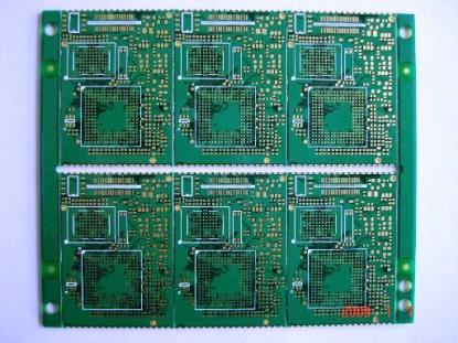
Layer Count: 8L Board Thickness: 1.0mm Panel Dimension:190*86mm/2up Material: S1141 Copper on board surface: 35μm Min Hole Diameter: 0.1mm Min line Width/Space: 8/8mil Surface Finish: ENIG+Selective OSP in BGA area This quick turn PCB is manufacture
Materials: FR-4 Layer count: 8 layers;40 mil thick Microvia (Laser drill) : 4 mil Min. line: 3 mil Application: Wireless LAN Card Finishing: Immersion gold

Materials: FR-4 Layer count: 8 layers;40 mil thick Microvia (Laser drill) : 4 mil Min. line: 3 mil Application: Wireless LAN Card Finishing: Immersion gold

MLT provides rigid and flexible circuit laser services including laser routing (excising), cavity skiving, coverlay/coverfilm routing, microvia drilling, ZIF Contours, Kapton window skives, depaneling, and marking. With 20 years experience, MLT has
Double-Sided & Multi-Layer PCB Material: - FR-4 / Hi-Temp FR-4 / FR-5 / G10 / BT / Polyimide - Very Thin PCB: 0.004" 2L ~ 0.030" 8L - Thick Copper: 1/4 oz. ~ 11 oz. Process: - PTH - Blind/Buried/Segmented Via - Sequential Lamination - MicroVia Capa
.jpg)
Quickturn PCB quote please sent E-mail to quotes@huanyupcb.com. HDI (High Density Intrerconnection) is defined as substrate or board with the Microvia of aperture below 6mil, hole pad below 0.25mm, connect pad density above 130 points / square inch

Quickturn PCB quote please sent E-mail to quotes@huanyupcb.com. HDI (High Density Intrerconnection) is defined as substrate or board with the Microvia of aperture below 6mil, hole pad below 0.25mm, connect pad density above 130 points / square inch
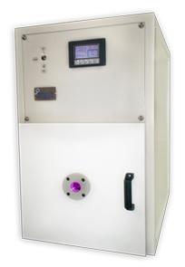
Compact Plasma Etcher The PE-100 is a complete system with vacuum pump designed to be reliable yet inexpensive enough to allow startup companies, medical labs and R&D facilities the opportunity to experience Plasma Etch technology. The all aluminum
Printed Circuit Board Design Service Bureau for high quality, low cost source for Printed Circuit Design, Training, Fabrication, and Project Management. While every job is unique, CA Design employs a battle-proven process for ensuring that your desi
Printed Circuit Board Design Service Bureau for high quality, low cost source for Printed Circuit Design, Training, Fabrication, and Project Management. While every job is unique, CA Design employs a battle-proven process for ensuring that your desi


