New Equipment | Fabrication Services
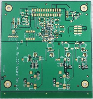
Minimum line width/space: 4mils Surface finish: immersion gold Board thickness: 1.60MM Minimum drilled hole diameter: 4mils Copper thickness: 0.5oz Special process : 0.25MM BGA , resin plugged vias in BGA pads
New Equipment | Surface Finish
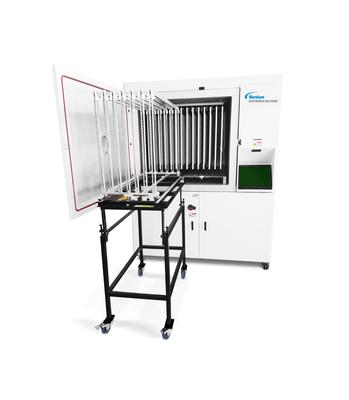
VIA Series plasma treatment systems offer superior plasma treatment uniformity for printed circuit board (PCB) panels. The MaxVIA, MaxVIA-Plus, and ModVIA systems deliver various plasma cleaning, surface activation, and adhesion improvement capabil

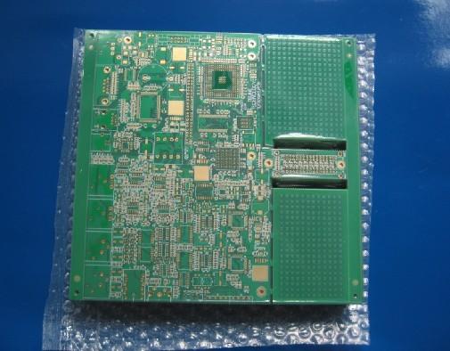
Project Description | Parameters 10 Layer (3 Stage) Thickness: 1.6+/-0.16 mm Min Hole Size: Via: 0.25 mm Blind Via: 0.15mm Width/Space: 0.1mm/0.08 mm Surface Treatment: ENIG | Craft 3 Stage HDI | Application Industrial Contr
Up to 30 layers, down to 3 mil traces / spaces, 6 mil drilled holes. MIL-P-55110 approved for FR-4, polyimide, PTFE, epoxy Thermount(tm). Copper Sealed Vias are available. Deliveries down to 24 hours are available.
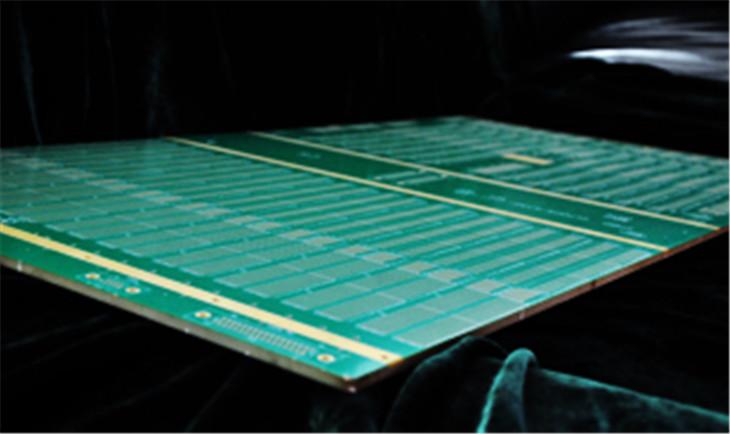
1. FR-4 Tg170 2. 20 layer, 1.6mm thick 3. 1 oz copper finished 4. 10% impedance control 5. Blind/buried vias 6. 0.1mm holes, HDI 7. Application: telecommunication, industrial control, medical equipment
New Equipment | Assembly Services
4 layer PCB Material: Rogers 5880 Finished Thickness :2.0 mm; Copper thickness : 1OZ finished ; Surface finishing: Immersion Tin Min Via hole size :0.30mm; Min Trace width/ spacing : 0.13 mm / 0.13 mm
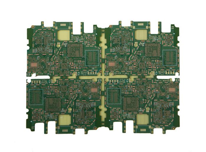
Project Description | Parameters 32 Layer Thickness: 6.2+/-0.62 mm Size: 870*540mm Min Hole Size: Via: 0.65 mm Width/Space: 0.1mm/0.15 mm Surface Treatment: ENIG | Craft 32 Layer Unsymmetrical Layup Strcture | Application Base Station
Project Description | Parameters 10 Layer (2 Stage) Thickness: 2.0+/-0.2 mm Min Hole Size: Via: 0.2 mm Blind Via: 0.1mm Width/Space: 0.08mm/0.08 mm Surface Treatment: ENIG | Craft 2 Stage BVH | Application Industrial Control
Bicheng provides impedance controlled PCB's for R&D, high-tech, IT research companies and organizations, large or small. Technical parameters *Controlled dielectric *Controlled impedance *Design coupons *Test coupons *Po

New Equipment | Fabrication Services
RF & Microwave PCB's ACI is a leader in providing complex RF/Microwave PCB’s covering a wide spectrum of product types including Defense/Aerospace, Medical Device, Imaging, and Telecommunications Equipment. ACI supports a wide range of frequency ban


