Industry News | 2008-03-12 15:38:55.0
Fine Line Stencil invites visitors to stop by booth 243 at APEX 2008 to learn about its recent positive changes in technology. The APEX exhibition and conference is scheduled to take place April 1-3, 2008 in Las Vegas.
Tronixlink's Electronic Contract Manufacturing Service (EMS) PCBA layout Prototype builds Printed Circuit Board Assembly (PCBA) - Single sided , Double sided , Multilayer, Backplanes, Industrial Power boards, Wire Wrap boards, Fine-line , Analog ,
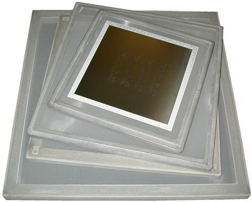
New Equipment | Solder Paste Stencils
Fine Line Stencil is a technology leading manufacture, committed to delivering the highest quality laser stencils in the industry. We use the most advanced laser and material technologies available in the world to meet current and future industry de
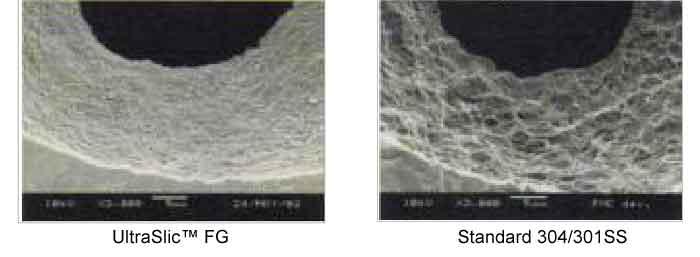
Fine Line Stencil’s new UltraSlic™ FG solder paste stencil is the latest breakthrough in stencil technology. With superior paste release below surface area ratios of 0.5, UltraSlic™ FG outperforms all other existing stencil technologies on the market
Fine Line Stencil's unique Slic Blade™ process uses electroformed nickel to form a hard, very smooth surface with extremely low surface energy (high lubricity). Solder paste readily sticks to most metal surfaces, even coated blades, due to metal's hi
Industry News | 2008-10-12 22:42:17.0
COLORADO SPRINGS, CO � October 2008 � FINE LINE STENCIL, a division of FCT Assembly and a leading manufacturer of stencil products, announces the promotion of Firas Dahgmash as CAD Manager.
Industry News | 2008-10-20 20:23:29.0
COLORADO SPRINGS, CO � October 20, 2008 � FINE LINE STENCIL, a division of FCT Assembly and a leading manufacturer of stencil products, announces that customers may now order online via its new Web site.
Industry News | 2013-04-29 09:50:51.0
Fine Line Stencil, a division of FCT Assembly, announces plans to hold an open house at its new facility in Richardson, TX.
Technical Library | 2021-06-21 19:34:02.0
In this era of electronics miniaturization, high yield and low-cost integrated circuit (IC) substrates play a crucial role by providing a reliable method of high density interconnection of chip to board. In order to maximize substrate real-estate, the distance between Cu traces also known as line and space (L/S) should be minimized. Typical PCB technology consists of L/S larger than 40 µ whereas more advanced wafer level technology currently sits at or around 2 µm L/S. In the past decade, the chip size has decreased significantly along with the L/S on the substrate. The decreasing chip scales and smaller L/S distances has created unique challenges for both printed circuit board (PCB) industry and the semiconductor industry. Fan-out panel-level packaging (FOPLP) is a new manufacturing technology that seeks to bring the PCB world and IC/semiconductor world even closer. While FOPLP is still an emerging technology, the amount of high-volume production in this market space provide a financial incentive to develop innovative solutions in order to enable its ramp up. The most important performance aspect of the fine line plating in this market space is plating uniformity or planarity. Plating uniformity, trace/via top planarity, which measures how flat the top of the traces and vias are a few major features. This is especially important in multilayer processing, as nonuniformity on a lower layer can be transferred to successive layers, disrupting the device design with catastrophic consequences such as short circuits. Additionally, a non-planar surface could also result in signal transmission loss by distortion of the connecting points, like vias and traces. Therefore, plating solutions that provide a uniform, planar profile without any special post treatment are quite desirable.
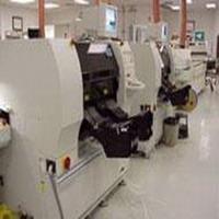
Industry News | 2008-06-11 18:29:34.0
COLORADO SPRINGS, CO � June 11, 2008 � FINE LINE STENCIL, a division of FCT Assembly and a leading manufacturer of stencil products, announces enhanced quality with investment in AOI equipment


.png)

