Career Center | Oldsmar, Florida USA | Engineering,Maintenance,Production
Job Title: Assembler 2 – IPC 610 – 1st Shift Address: 3655 Tampa Rd, Oldsmar FL 34677 Duration: 1 year Pay Rate: $15-$18 Hours: 9/80 schedule Monday – Thursday 6:00AM – 3:30PM, Friday 6:00AM to 2:30PM Job Description: Use microscope to verify
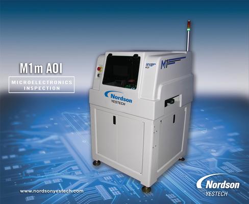
3550 sq. mm second (> 5.5 sq. in / second) Maximum Board Size: 350mm x 250mm (14 x 10 in.) Minimum Board Size: 50mm x 50mm (2 x 2 in.) Topside Clearance: 25mm (1 in.) Bot
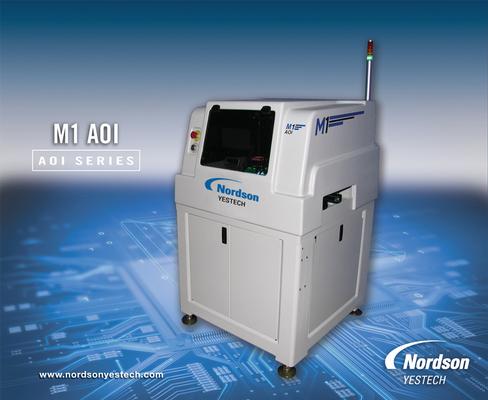
3550 sq. mm second (> 5.5 sq. in / second) Maximum Board Size: 350mm x 250mm (14 x 10 in.) Minimum Board Size: 50mm x 50mm (2 x 2 in.) Topside Clearance: 25mm (1 in.) Bot
New Equipment | Test Equipment
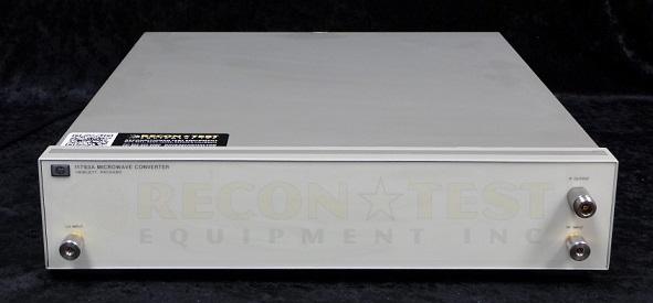
The Agilent 11793A microwave converter downconverts microwave signals to the frequency range of the Agilent 8902A measuring receiver. For signals above 1.3 GHz, the 11793A routes the signal through its internal mixer. Below 1.3 GHz, signals are route
Training Courses | | | PCB Rework and Hand Soldering Courses
The PCB rework and hand soldering courses courses cover techniques of rework and repair of PCBs, BGAs and other electronics assemblies, and teach fundamentals of soldering of electronics assemblies.
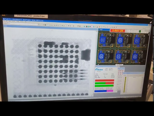
This is a demonstration of the YESTech YTX-X3 3D X-Ray inspecting pcbs in production. This YTX-X3 is available at the Capital Equipment Exchange. https://www.ce-exchange.com/details/?product=7426&pn=YESTech-YTX-X3-3D-X-Ray
Technical Library | 2014-06-05 16:44:07.0
Stencil printing capability is becoming more important as the range of component sizes assembled on a single board increases. Coupled with increased component density, solder paste sticking to the aperture sidewalls and bottom of the stencil can cause insufficient solder paste deposits and solder bridging. Yield improvement requires increased focus on stencil technology, printer capability, solder paste functionality and understencil cleaning.(...) The purpose of this research is to study the wipe sequence, wipe frequency and wipe solvent(s) and how these factors interact to provide solder paste printing yield improvement.
Technical Library | 2016-11-30 21:30:50.0
Mid-chip solder balling is a defect typically associated with solder paste exhibiting poor hot slump and/or insufficient wetting during the reflow soldering process, resulting in paste flowing under the component or onto the solder resist. Once molten, this solder is compressed and forced to the side of the component, causing mid-chip solder balling.This paper documents the experimental work performed to further understand the impact on mid-chip solder balling from both the manufacturing process and the flux chemistry.
Technical Library | 2017-08-17 12:28:30.0
At SMT assembly, flux outgassing/drying is difficult for devices with poor venting channel, and resulted in insufficiently dried/burnt-off flux residue for no-clean process. Examples including: Large low stand-off components such as QFN, LGA Components covered under electromagnetic shield which has either no or few venting holes Components assembled within cavity of board Any other devices with small open space around solder joints
Technical Library | 2023-05-02 19:16:57.0
1.5 with a 150μm specification window. For 0201 components, the minimum requirement is CpK > 2.0 with a 100μm specification window. The spec window may need to be reduced down to 75μm if the controls for high volume manufacturing are insufficient. Also directly impacting the placement quality is the ability to apply sufficient solder consistently to the board. The goal is to maintain current printing practices, but the effect of powder size will be examined. This paper will evaluate the impact of placement accuracy and solder powder size on 0201 manufacturing quality.


.gif)