New Equipment | Solder Materials
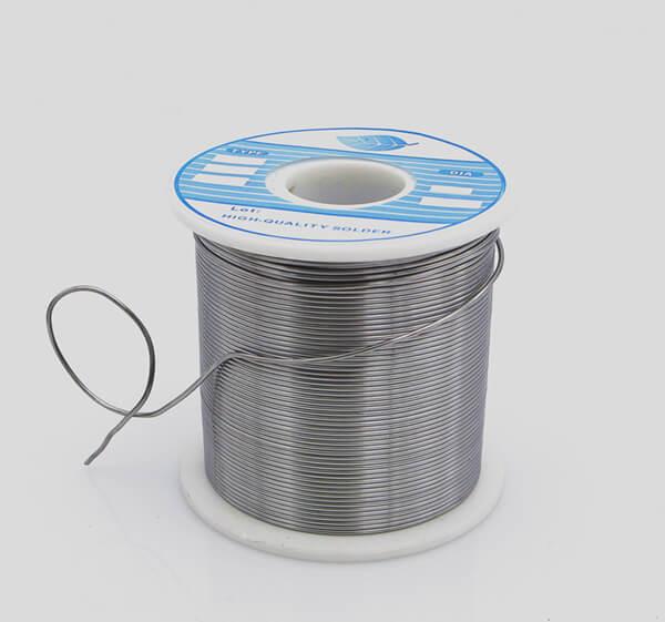
http://www.flason-smt.com/product/Customizable-0-3-5-0mm-diameter-sn42bi58-lead-free-solder-wire.html Customizable 0.3-5.0mm diameter sn42bi58 lead free solder wire lead free solder wire sn42bi58 0.3-5.0mm diameter Customizable Product descri
Technical Library | 2017-08-17 12:28:30.0
At SMT assembly, flux outgassing/drying is difficult for devices with poor venting channel, and resulted in insufficiently dried/burnt-off flux residue for no-clean process. Examples including: Large low stand-off components such as QFN, LGA Components covered under electromagnetic shield which has either no or few venting holes Components assembled within cavity of board Any other devices with small open space around solder joints
Technical Library | 2015-02-12 16:57:56.0
Electronic systems are known to be affected by the environmental and mechanical conditions, such as humidity, temperature, thermal shocks and vibration. These adverse environmental operating conditions, with time, could degrade the mechanical efficiency of the system and might lead to catastrophic failures.The aim of this study is to investigate the mechanical integrity of lead-free ball grid array (BGA) solder joints subjected to isothermal ageing at 150°C for up to 1000 hours. Upon ageing at 150°C the Sn-3.5Ag solder alloy initially age-softened for up to 200 hours. This behaviour was linked to the coarsening of grains. When aged beyond 200 hours the shear strength was found to increase up to 400 hours. This age-hardening was correlated with precipitation of hard Ag3Sn particles in Sn matrix. Further ageing resulted in gradual decrease in shear strength. This can be explained as the combined effect of precipitation coarsening and growth of intermetallic layer. The fractured surfaces of the broken solder balls were also investigated under a Scanning Electron Microscope. The shear failures were generally due to ductile fractures in bulk solders irrespective of the ageing time.
Technical Library | 2016-11-30 21:30:50.0
Mid-chip solder balling is a defect typically associated with solder paste exhibiting poor hot slump and/or insufficient wetting during the reflow soldering process, resulting in paste flowing under the component or onto the solder resist. Once molten, this solder is compressed and forced to the side of the component, causing mid-chip solder balling.This paper documents the experimental work performed to further understand the impact on mid-chip solder balling from both the manufacturing process and the flux chemistry.
Industry News | 2010-12-10 12:27:00.0
Ironwood Electronics recently introduced a new spring pin socket addressing precise resistance measurement need for testing power management devices - SSK-QFN-7000.
Parts & Supplies | Repair/Rework
Three independent heaters control systems. FG-P6000 is available heating portion of the PCB board by hot-air circulate both from top and bottom at the same time. With large IR bottom heating, it can completely avoid PCB deformation during reworking
Career Center | Sherman, Texas USA | Engineering,Production,Research and Development,Technical Support
SMT Packaging Engineer: Location: Texas - Sherman , TX Group: HVAL Degree Requirements: BS ME/ChemE/Materials The person in this position will have the ability to make very significant financial contributions to TI because this is a very critic
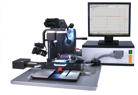
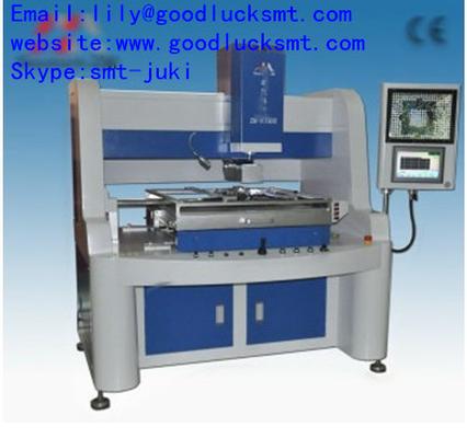
New Equipment | Rework & Repair Equipment
Cost Effective Rework of Medium Size Boards The FINEPLACER® coreplus is a compact, yet versatile rework system that offers a level of professionalism that exceeds its attractive price. The system offers proven rework technology for a wide spectrum
Technical Library | 2019-08-07 22:56:45.0
The requirement to reconsider traditional soldering methods is becoming more relevant as the demand for bottom terminated components (QFN/BTC) increases. Thermal pads under said components are designed to enhance the thermal and electrical performance of the component and ultimately allow the component to run more efficiently. Additionally, low voiding is important in decreasing the current path of the circuit to maximize high speed and RF performances. The demand to develop smaller, more reliable, packages has seen voiding requirements decrease below 15 percent and in some instances, below 10 percent.Earlier work has demonstrated the use of micro-fluxed solder preforms as a mechanism to reduce voiding. The current work builds upon these results to focus on developing an engineered approach to void reduction in leadless components (QFN) through increasing understanding of how processing parameters and a use of custom designed micro-fluxed preforms interact. Leveraging the use of a micro-fluxed solder preform in conjunction with low voiding solder paste, stencil design, and application knowhow are critical factors in determining voiding in QFN packages. The study presented seeks to understand the vectors that can contribute to voiding such as PCB pad finish, reflow profile, reflow atmosphere, via configuration, and ultimately solder design.A collaboration between three companies consisting of solder materials supplier, a power semiconductor supplier, and an electronic assembly manufacturer worked together for an in-depth study into the effectiveness of solder preforms at reducing voiding under some of the most prevalent bottom terminated components packages. The effects of factors such as thermal pad size, finish on PCB, preform types, stencil design, reflow profile and atmosphere, have been evaluated using lead-free SAC305 low voiding solder paste and micro-fluxed preforms. Design and manufacturing rules developed from this work will be discussed.
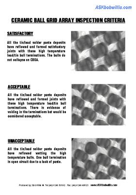
Ball Grid Array X-Ray Inspection Guide - 20 Colour Charts Includes X-Ray inspection guide of satisfactory BGA solder joints and process defects, x-ray images are black and white. The posters are provided as a pdf file and can be printed as A4 or A3


