New Equipment | Coating Materials
This kit contains 10 packages of clear, low viscosity, superior strength epoxy, precisely measured out into two-compartment plastic packages so it's easy to use and there's no measuring. Once cured, this epoxy makes an effective electrical insulator
New Equipment | Test Equipment
Military-style laboratory services to validate bare boards for product assurance. Testing for delamination, voids, copper thickness, hole quality, proper stack-up, etc. Customer receives all cross-section pucks, boards and laboratory report with reco
Events Calendar | Tue Jan 23 00:00:00 EST 2018 - Tue Jan 23 00:00:00 EST 2018 | New Milford, Connecticut USA
FREE Webinar: Eliminate Circuit Board Problems and Failure Modes
Industry Directory | Manufacturer
The leading provider of easy to apply nano-tech surface modification technologies.
Industry Directory | Manufacturer
CSM Instruments develops, manufactures and sells instruments to characterize mechanical properties of surfaces. We have been the world leader in this market for more than 30 years.
Technical Library | 2016-05-12 16:29:40.0
Advances in miniaturized electronic devices have led to the evolution of microvias in high density interconnect (HDI) circuit boards from single-level to stacked structures that intersect multiple HDI layers. Stacked microvias are usually filled with electroplated copper. Challenges for fabricating reliable microvias include creating strong interface between the base of the microvia and the target pad, and generating no voids in the electrodeposited copper structures. Interface delamination is the most common microvia failure due to inferior quality of electroless copper, while microvia fatigue life can be reduced by over 90% as a result of large voids, according to the authors’ finite element analysis and fatigue life prediction. This paper addresses the influence of voids on reliability of microvias, as well as the interface delamination issue.
Technical Library | 2024-09-02 17:31:09.0
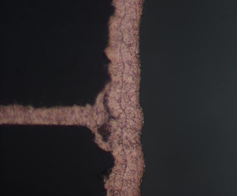
The cracking and delamination of printed circuit boards (PCB) during exposure to elevated thermal exposure, such as reflow and rework, have always been a concern for the electronics industry. However, with the increasing spread of Pb-free assembly into industries with lower volume and higher complexity, the occurrence of these events is increasing in frequency. Several telecom and enterprise original equipment manufacturers (OEMs) have reported that the robustness of their PCBs is their number one concern during the transition from SnPb to Pb-free product. Cracking and delamination within PCBs can be cohesive or adhesive in nature and can occur within the weave, along the weave, or at the copper/epoxy interface (see Figure 1). The particular role of moisture absorption and other PCB material properties, such as out of plane expansion on this phenomenon is still being debated.
Technical Library | 2024-02-05 17:51:01.0
Objective: Drying = reducing the humidity in PCB before soldering Preventing delamination caused by thermal stress after moisture absorption Methods: Drying in convection and/ or vacuum oven Parameters subject to material type, soldering surface, layer count, time to soldering, layout (copper-plated areas)
Training Courses | | | IPC-600 Specialist (CIS)
The Certified IPC-600 Specialist (CIS) training targets quality assurance and acceptance of bare printed circuit boards.
Technical Library | 2024-09-02 18:48:58.0
The conversion to higher temperature "Lead Free" assembly reflow conditions has created an increased awareness that entrapped or absorbed moisture is a frequent root cause of thermally induced delamination at assembly reflow. There are two connected failure modes from entrapped moisture; incomplete resin cross-linking resulting in premature resin decomposition and also severe Z axis expansion from "explosive vaporization of the entrapped moisture at elevated temperatures at assembly reflow". Ultimately, both result in delamination failure. Other papers have shown the negative effects of entrapped moisture before lamination including delamination, red color, reduced thermal reliability and increased high speed signal loss. In this paper, various materials were tested for moisture sensitivity during lamination. Tests were performed at varying lamination conditions including a pre-vacuum step and "kiss" step. Pressure and cure temperature parameters were evaluated for minimizing or eliminating the effect of trapped moisture. Also included are the results of inner layer moisture removal baking conditions and their effect on peel strength and thermal reliability.


