Industry News | 2010-06-30 12:09:49.0
MARTIN will demonstrate the Reball / Prebump 03.1 unit at the upcoming SMTA Ohio Valley Expo & Tech Forum, scheduled for Wednesday, July 14, 2010 at the Doubletree Hotel in Cleveland, OH. This standalone unit is an easy and cost effective solution for BGA reballing and QFN solder bumping.
New Equipment | Rework & Repair Equipment
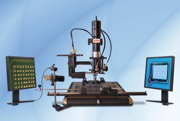
The PDR E3S SMD Rework Station offers dual closed loop feedback for advanced BGA Repair, QFN Repair, Flip Chip Repair, DFN repair, QFP's, SOIC's and more, and is is engineered with only the finest materials and components for optimum precision and r
New Equipment | Rework & Repair Equipment
FINEPLACER® pico rs is an enhanced hot air rework station for assembly and rework of all types of SMD components. The system is a best seller for professional mobile device rework in high density environments. A high level of process modularity allo
Technical Library | 2018-09-26 20:33:26.0
Bottom terminated components, or BTCs, have been rapidly incorporated into PCB designs because of their low cost, small footprint and overall reliability. The combination of leadless terminations with underside ground/thermal pads have presented a multitude of challenges to PCB assemblers, including tilting, poor solder fillet formation, difficult inspection and – most notably – center pad voiding. Voids in large SMT solder joints can be difficult to predict and control due to the variety of input variables that can influence their formation. Solder paste chemistries, PCB final finishes, and reflow profiles and atmospheres have all been scrutinized, and their effects well documented. Additionally, many of the published center pad voiding studies have focused on optimizing center pad footprint and stencil aperture designs. This study focuses on I/O pad stencil modifications rather than center pad modifications. It shows a no-cost, easily implemented I/O design guideline that can be deployed to consistently and repeatedly reduce void formation on BTC-style packages.

New Equipment | Rework & Repair Equipment
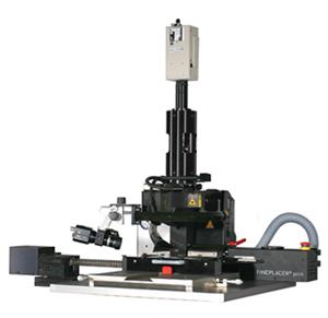
Ultimate Performance, BGA Rework Station for small-large PCBs up to 24"/620mm The PDR E6 XL BGA Rework Station is made of only the finest materials and components for optimum precision and rework excellence. PDR's E6 SMD Rework Station is PDR's larg
Technical Library | 2015-07-14 13:19:10.0
Bottom terminated components (BTC) are leadless components where terminations are protectively plated on the underside of the package. They are all slightly different and have different names, such as QFN (quad flat no lead), DFN (dual flat no lead), LGA (land grid array) and MLF (micro lead-frame. BTC assembly has increased rapidly in recent years. This type of package is attractive due to its low cost and good performance like improved signal speeds and enhanced thermal performance. However, bottom terminated components do not have any leads to absorb the stress and strain on the solder joints. It relies on the correct amount of solder deposited during the assembly process for having a good solder joint quality and reliable reliability. Voiding is typically seen on the BTC solder joint, especially on the thermal pad of the component. Voiding creates a major concern on BTC component’s solder joint reliability. There is no current industry standard on the voiding criteria for bottom terminated component. The impact of voiding on solder joint reliability and the impact of voiding on the heat transfer characteristics at BTC component are not well understood. This paper will present some data to address these concerns.
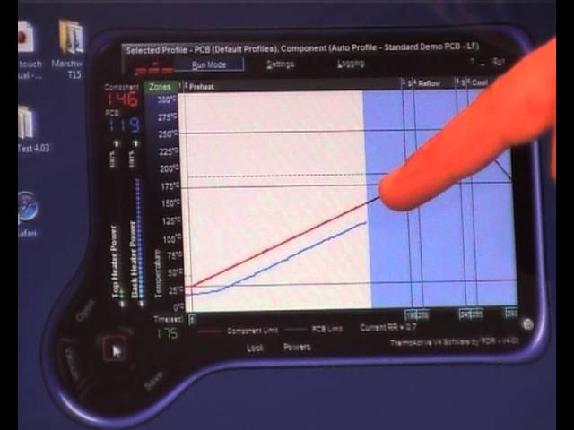
This is an indepth video showing you how to rework a BGA using the PDR IR-E3 with CCTV/Split prism vision alignment rework station from our Evolution series. We call this system the E3Vi For further details on PDR Focused IR rework stations/systems
Technical Library | 2015-12-31 15:19:28.0
Today's consumer electronic product are characterized by miniatuization, portability and light weight with high performance, especially for 3G mobile products. In the future more fine pitch CSPs (0.4mm) component will be required. However, the product reliability has been a big challenge with the fine pitch CSP. Firstly, the fine pitch CSPs are with smaller solder balls of 0.25mm diameter or even smaller. The small solder ball and pad size do weaken the solder connection and the adhesion of the pad and substrate, thus the pad will peel off easily from the PCB substrate. In addition, miniature solder joint reduce the strength during mechanical vibration, thermal shock, fatigue failure, etc. Secondly, applying sufficient solder paste evenly on the small pad of the CSP is difficult because stencil opening is only 0.25mm or less. This issue can be solved using the high end type of stencil such as Electroforming which will increase the cost.
Industry News | 2009-03-18 17:08:59.0
FINETECH will demonstrate today's most requested advanced rework applications in booth #2059 at the upcoming APEX 2009, scheduled to take place March 31 � April 2, 2009 at the Mandalay Bay Convention Center in Las Vegas.
Industry News | 2014-05-22 11:36:25.0
Indium Corporation's Derrick Herron, technical support engineer, will serve as an expert presenter at ZESTRON’s Assembly, Cleaning, and Reliability Hands-on Workshop on June 10 in Franklin, Mass.


.png)