This system is purpose built for volume inspection in a production environment, either in semiconductor packaging or PCB assembly. With a sample scan area of up to 350 x 530mm, the cabinet can accommodate large samples or t
Nanovea 3D Non-Contact Profilometers are designed with leading edge optical pens using superior white light axial chromatism. Nano through macro range is obtained during measurement (Profile Dimension, Roughness Finish Texture, Shape Form Topography,
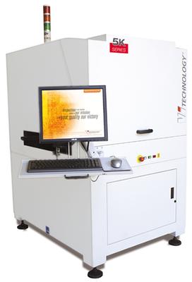
The large board solution The 5K Series offers flexibility for wider board applications and benefits from all the latest Vi TECHNOLOGY® innovations, including Selective 3D AOI technology for accurate tilt and coplanarity measurement of ICs, connector
New Equipment | Solder Materials
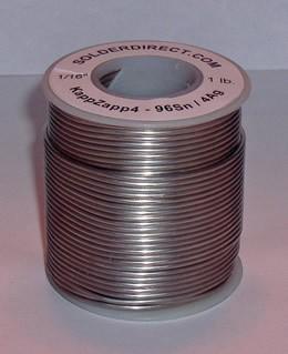
The KappZapp4 - 4% Silver formula is often preferred for hand soldering Stainless and Copper parts. It has a wider slushy or plastic range to allow users to manipulate parts during cooling. Low melting temperatures prevent loss of properties and mi
New Equipment | Test Equipment
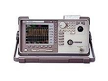
The Agilent 86143B is a portable optical spectrum analyzer for 50 GHz applications. The 86143B maintains most of the higher performance characteristics of the 86142B/86145B models while providing measurement solutions at value prices. This OSA has al
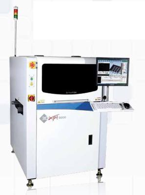
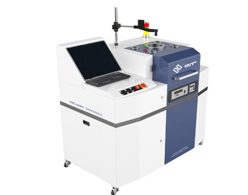
Technical Innovation The first 10 bit image processing in its industry by on-the-fly vibrationless scan (High speed & high precision image acquisition) 4 times higher height measurement resolution than the existing Moire technology (The best
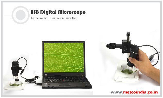
We take our opportunity to introduce you one of our latest and Imported Products USB Digital microscopes to you. Download Here USB Digital Microscope Product Catalogue Relevant catalogue enclosed gives all the technical details. What is a digit
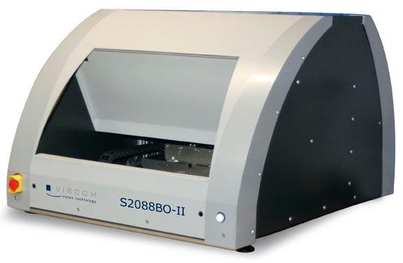
This compact AOI system was developed to inspect medium and small product runs. During inspection, a high-resolution camera records all bond sites and wires. Dies, bond sites, wire course and component position are only a part of the inspection scope
New Equipment | Rework & Repair Equipment
This unique rework stenciling system is very simple to use. Adhesive Backed Stencil Thickness: 004in (.10mm), .005in (.13mm) and .006in (.15mm) Minimum Aperture Size: .002in (.05mm) Stencil Material: Plastic film with release liner. The adhesive bac
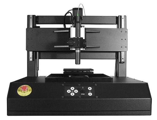
New Equipment | Soldering - Other
Sunny Company:Beijing Chengliankaida Technology Co.,Ltd Address : SanCang Road Sanjianfang airport ,Tongzhou district , Beijing China Email: salemachines@bjclkdkj.cn Skype :smdsupplier Whatsapp: +86 159 01434496 Wechat: + 86 159 0143 4496


