Training Courses | | | PCB Design Courses
The PCB design courses teach students the process, techniques and tools needed to design layout of printed circuit boards.
Technical Library | 2020-02-05 18:20:06.0
Consortium Projects - Thermal Cycling Reliability Consortium projects allow for joint research to investigate the reliability of multiple solder alloys under a variety of environmental stress conditions. Project jointly sponsored by iNEMI and HDP User Group and including CALCE and Universal consortium currently assessing 15 third-generation solder alloys..
Industry News | 2004-09-27 18:00:54.0
Compared with the standard CAMs provided with the AnadigmDesigner�2 EDA tool used for programming FPAAs, the new Customer Collection CAMs implement more complex, application-specific functions.
Parts & Supplies | General Purpose Equipment
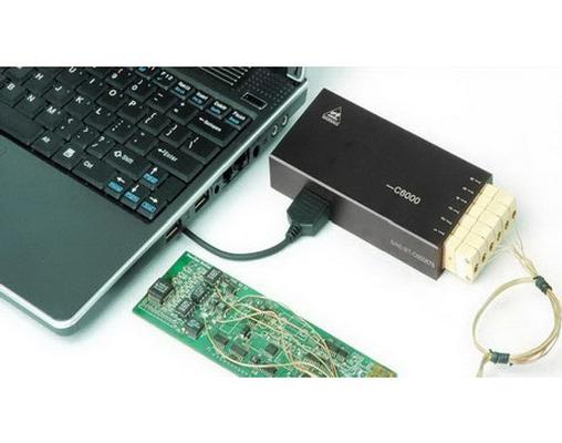
FEATHERS 1. Efficiency, collect data continuously for 16 times and forward to computer to analysis grouping; 2. It is available base on PC (WINDOWS) and PDA(Pocket) to analyze; 3. Low power, use lithium battery that can k
Industry News | 2004-08-17 16:12:29.0
Participants will experience a hands-on, small-group setting in which they can start designing and implementing complex analog circuits with Field Programmable Analog Arrays (FPAAs).
Technical Library | 2016-03-24 17:37:09.0
Today's Electronic Industry is changing at a high pace. The root causes are manifold. So world population is growing up to eight billions and gives new challenges in terms of urbanization, mobility and connectivity. Consequently, there will raise up a lot of new business models for the electronic industry. Connectivity will take a large influence on our lives. Concepts like Industry 4.0, internet of things, M2M communication, smart homes or communication in or to cars are growing up. All these applications are based on the same demanding requirement – a high amount of data and increased data transfer rate. These arguments bring up large challenges to the Printed Circuit Board (PCB) design and manufacturing.This paper investigates the impact of different PCB manufacturing technologies and their relation to their high frequency behavior. In the course of the paper a brief overview of PCB manufacturing capabilities is be presented. Moreover, signal losses in terms of frequency, design, manufacturing processes, and substrate materials are investigated. The aim of this paper is, to develop a concept to use materials in combination with optimized PCB manufacturing processes, which allows a significant reduction of losses and increased signal quality.
Technical Library | 2019-02-20 16:35:24.0
The High Density Packaging (HDP) User Group has completed a project evaluating the high frequency loss impacts of a variety of imaged core surface treatments (bond enhancement treatments, including chemical bonding and newer low etch alternative oxides) applied just prior to press lamination. Initial high frequency Dk/Df electrical test results did not show a strong correlation with any of the methods utilized within this project to measured surface roughness. The more significant factor affecting the measured loss is the choice of pre-lamination surface treatment. Most of the new chemical treatment systems outperform the older existing systems which depend upon surface roughness techniques to promote adhesion.
Parts & Supplies | Repair/Rework
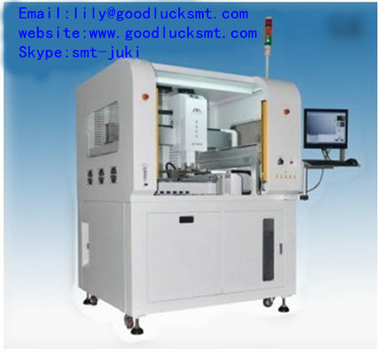
. This machine adopts industrial computer control, full automatic vision alignment system can acquire BGA and the PCB image through the CCD camera and collect them on the image positioning processing system, calculate the offset position and angle th
Industry News | 2009-10-09 01:31:11.0
With realization of the importance that price plays in the selection of PCB assembly equipment, www.manncorp.com has been redesigned to furnish a quotation on any product within five seconds. This landmark feature, reportedly unique to Manncorp, is activated whenever the five-second digital timer – appearing on every product page – is clicked. As soon as the user provides the brief identification information required, the countdown begins as the requested quote is instantly processed and e-mailed.
Technical Library | 2017-10-12 15:45:25.0
The risk associated with whisker growth from pure tin solderable terminations is fully mitigated when all of the pure tin is dissolved into tin-lead solder during SMT reflow. In order to take full advantage of this phenomenon, it is necessary to understand the conditions under which such coverage can be assured. A round robin study has been performed by IPC Task group 8-81f, during which identical sets of test vehicles were assembled at multiple locations, in accordance with IPC J-STD-001, Class 3. All of the test vehicles were analyzed to determine the extent of complete tin dissolution on a variety of component types. Results of this study are presented together with relevant conclusions and recommendations to guide high reliability end-users on the applicability and limitations of this mitigation strategy.

A global industrial auction and valuation business with extensive experience in SMT, PCB Assembly & Manufacturing, Test, Semiconductor and other Electronics Machinery & Equipment.
Manufacturer / Equipment Dealer / Broker / Auctions
896 Main Street
Branford, CT USA
Phone: 203-488-7020


