New Equipment | Fabrication Services
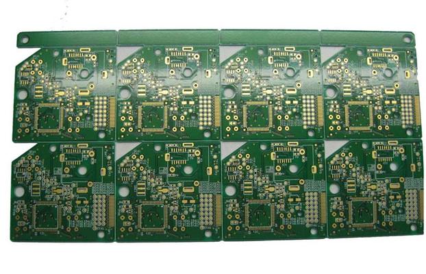
Low Cost Heavy Copper PCB China 4 Layers Circuit Boards Supplier Quick Details: FR4 base material 1.6mm board thickness 2oz heavy copper Plating gold finishing RF custom PCB boards Used for Radio Frequency From China PCB manufacturer Specifications
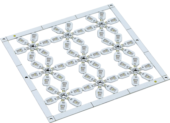
New Equipment | Assembly Services
Quick turn Prototype PCBs from 24 hour turnaround to high volume printed circuit board production from our domestic plant in USA and/or China facilities. Our Modern 38,000 sq. ft. manufacturing plant with multi-million dollar investment with latest e
Industry News | 2020-10-04 15:41:30.0
MacDermid Alpha Electronics Solutions will be exhibiting at the Taiwan Printed Circuit Association (TPCA) exhibition and presenting two technical papers at the IMPACT-EMAP Conference, co-located with TPCA in Taipei, October 21-23, 2020. The papers detail some of the ways in which MacDermid Alpha has invested in the research of innovative manufacturing processes to meet the demanding standards required for the new age of miniaturization.
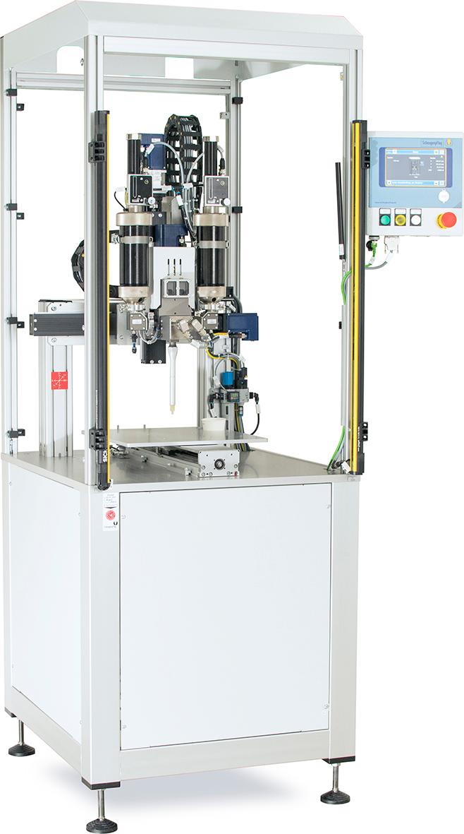
The system includes a 3-axis-system and a light curtain as well as the proven Dos P016 and the cartridge expulsion unit A90 C with filling level monitoring. Advantages Fast start of production Unrivaled service life Short delivery times Quick
Industry News | 2021-03-31 17:56:27.0
MacDermid Alpha Electronics Solutions will be a Supporting Partner at the upcoming IMAPS Device Packaging Conference being held virtually from April 12-15, 2021. MacDermid Alpha will highlight their entire portfolio of technologies from their MacDermid Enthone, Alpha, Kester, and Compugraphics brands essential to advanced semiconductor packaging and the markets it enables.
New Equipment | Fabrication Services
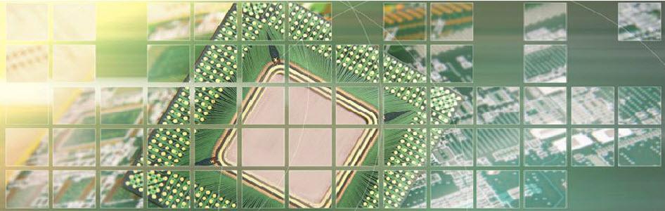
Multilayer PCB's ACI manufactures a wide variety of Multilayer PCB's for various applications spanning numerous industries and technologies. We can build your high layer count PCB's using a wide variety of high speed low loss materials from epoxies
Technical Library | 2023-01-10 20:15:42.0
Over the past years there has been consistent growth in the use of electroless nickel / immersion gold (ENIG) as a final finish. The finish is now frequently being used for PBGA, CSP, QFP and COB and more recently gathered considerable interest as a low cost under-bump metallization for flip chip bumping application. One of the largest users for this finish has been the telecommunication industry, were millions of square meters of PCBs with ENIG have been successfully used. The nickel layer offers advantages such as multiple soldering cycles and hand reworks without copper dissolution being a factor. The nickel also acts as a reinforcement to improve through-hole and blind micro via thermal integrity. In addition the nickel layer offers advantages such as co-planarity, Al-wire bondability and the use as contact surface for keypads or contact switching. Especially those pads, which are not covered by solder need a protective coating in corrosive environment – such as high humidity or pollutant gas.

Compact and optimised for simple Gluing and Dispensing Tasks The DesktopCell is a compact, integrated solution for small to medium-sized batches and for prototype production. It unites all the advantages of a fully fledged dispensing cell and a smal
New Equipment | Fabrication Services
Cheap PCB Manufacturing Fr4/CEM3 PCB The most common PCBs, for every PCB supplier, most cost-effective. High Tg PCB More heat resistant, better dimensional stability, PS is a PCB supplier of Tg130-190 boards (FR4).
Technical Library | 2022-12-05 16:28:06.0
The work evaluates the impact of latent heat (LH) absorbed or released by a solder alloy during melting or solidification, respectively, on changes of dimensions of materials surrounding of the solder alloy. Our sample comprises a small printed circuit board (PCB) with a blind via filled with lead-free alloy SAC305. Differential scanning calorimetry (DSC) was employed to obtain the amount of LH per mass and a thermomechanical analyzer was used to measure the thermally induced deformation. A plateau during melting and a peak during solidification were detected during the course of dimension change. The peak height reached 1.6 μm in the place of the heat source and 0.3 μm in the distance of 3 mm from the source. The data measured during solidification was compared to a numerical model based on the finite element method. An excellent quantitative agreement was observed which confirms that the transient expansion of PCB during cooling can be explained by the release of LH from the solder alloy during solidification. Our results have important implications for the design of PCB assemblies where the contribution of recalescence to thermal stress can lead to solder joint failure.


